The 4th and final installment of a Chromis Technologies series on using AFPs for precise surface control
Introduction
In this series, we’ve been exploring how amorphous fluoropolymers (AFPs) give engineers the ability to control surfaces with extraordinary precision. We started with the fundamentals of surface engineering, then looked at how AFPs tune wettability, and most recently, how they enable electrowetting on dielectric (EWOD) systems.
Now, we turn to one of the most exciting frontiers where all of this comes together: digital microfluidics (DMF). These platforms are reshaping laboratory automation, with the ability to manipulate nanoliter droplets with precision – on a chip smaller than a credit card – turning what used to be complex lab protocols into compact, automated platforms. From drug discovery and synthetic biology to point-of-care diagnostics and environmental monitoring, DMF is transforming the way complex experiments and tests are performed.
Central to these advances are the materials that make reliable electrowetting possible. Two leading AFPs – CYTOP® and Teflon AF™ – have been studied extensively for their combination of dielectric strength, hydrophobicity, and durability that DMF devices demand. In this article, we’ll look at the science behind their performance, highlight what the research shows, and explain why AFPs are the unsung enablers of the lab-on-a-chip revolution.
How AFPs Power Digital Microfluidics and Lab-on-a-Chip Innovation
Digital microfluidics is one of the most promising platforms for miniaturized laboratory automation. By controlling droplets in the nanoliter-to-microliter range with electric fields, DMF eliminates bulky pumps and channels. Instead, droplets can be created, moved, split, and merged programmatically. This capability makes DMF the backbone of many next-generation lab-on-a-chip devices, from point-of-care diagnostics to drug discovery tools.
The dielectric surface material is the critical enabler of DMF device performance. Without robust, reliable electrowetting layers, droplets cannot be manipulated with the precision or durability required for real-world applications. That’s where amorphous fluoropolymers like CYTOP and Teflon AF come in.
What is Digital Microfluidics?
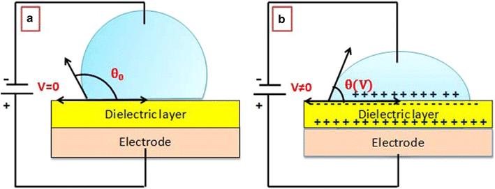
DMF is a fluid-handling technology that manipulates droplets through electrowetting on dielectric. When a voltage is applied beneath a dielectric/hydrophobic layer, the droplet’s contact angle changes, allowing it to move across an electrode array. By selectively energizing electrodes, droplets can be transported, dispensed, or mixed — creating reconfigurable workflows on a single platform.
DMF systems can automate laboratory workflows such as:
- Sample preparation
- Enzymatic reactions
- Cell culture
- PCR and gene editing
- Diagnostic assays
One chip can execute many protocols — from PCR amplification to single-cell isolation — with high precision and minimal reagent use.
Why Surface Materials Matter in DMF
For EWOD to function, the dielectric/hydrophobic topcoat must strike a delicate balance:
- Dielectric strength to prevent breakdown under high voltages.
- Low surface energy for consistent droplet mobility.
- Chemical resistance to prevent fouling by biological fluids and solvents.
- Durability to withstand thousands of actuation cycles without degrading.
- Optical clarity for fluorescence detection or microscopy.
In the absence of these properties, failure at the surface layer leads to unreliable droplet control, contamination, or total device failure.
Research has shown that AFPs are among the most effective materials at meeting these stringent requirements.
Research Insights: CYTOP and Teflon AF in EWOD
Extensive studies confirm the performance advantages of AFPs for EWOD:
- Low-voltage operation: Sub-20 nm films of Teflon AF and CYTOP enable actuation at 6–15 V, with contact angle modulation from 121°→81° (Teflon AF) and 114°→95° (CYTOP).
- Optimal thickness: A ~12 nm CYTOP film maintains ~110° contact angles but requires 80–90 V; thinner films reduce voltage but increase hysteresis.
- Composite approaches: CYTOP/Teflon AF bilayers achieve up to 120° contact angles with fast (~10 ms) switching and endurance up to breakdown voltages of 68–72 V.
- Durability: Studies show CYTOP degrades more slowly under DC operation than Teflon AF, with hydrophobicity recoverable through thermal annealing.
- Scalability: CYTOP has been used successfully in picoliter droplet actuation at voltages as low as 17–22 Vrms.
Together, these findings underscore why CYTOP and Teflon AF have become the go-to topcoat dielectrics in both research and commercial DMF platforms.
Applications Enabled by AFP-Based DMF
The use of AFP-coated EWOD devices is unlocking critical applications:
- Drug Discovery & Synthetic Biology – Automating screening, gene assembly, and micro-scale reactions.
- Diagnostics & PCR-on-Chip – Enabling rapid, point-of-care assays with minimal sample handling.
- Single-Cell Omics – Isolating and analyzing individual cells for genomics and proteomics.
- Environmental Monitoring – Detecting pollutants in portable, field-deployable devices.
- Newborn Screening – High-throughput testing for inherited metabolic diseases.
Each of these fields depends on stable, high-performance surfaces — which AFPs uniquely deliver.
The Future of Lab-on-a-Chip with AFPs
The future of DMF is moving rapidly toward scalable, manufacturable platforms. As devices become more complex and widely deployed, the importance of material science will only increase.
At Chromis Technologies, our CyclAFlor® family of materials builds on the foundation established by CYTOP and Teflon AF, delivering the dielectric strength, surface control, and durability needed to bring these devices from prototype to product.
Without AFPs, digital microfluidics would remain a laboratory curiosity. With them, it’s becoming a transformative technology.
Related Reading
Part 1: Surface Engineering with Amorphous Fluoropolymers
Part 2: Controlling Surface Energy and Wettability with AFPs
Part 3: The Electrowetting on Dielectric (EWOD) Properties and Applications of AFPs
Learn More
Interested in how amorphous fluoropolymers can advance your cutting-edge research or new product development? Our team at Chromis Technologies is here to help.
Contact us to learn more about our materials, capabilities, and how we can support your innovation initiatives.
References
Banpurkar, A. G., Sawane, Y. B., Wadhai, S. M., Murade, C. U., Sîretanu, I., van den Ende, D., & Mugele, F. (2017). Spontaneous electrification of fluoropolymer–water interfaces probed by electrowetting. Faraday Discussions, 199, 29. https://ris.utwente.nl/ws/files/30079588/Spontaneous_electrification.pdf
Chae, J. B., Kwon, J., Yang, J. S., Rhee, K., & Chung, S. (2013, January). Investigation on the thickness effect of a hydrophobic layer for operating voltage reduction in EWOD systems. In 2013 IEEE 26th International Conference on Micro Electro Mechanical Systems (MEMS) (pp. 1095–1098). https://doi.org/10.1109/MEMSYS.2013.6474444
Hou, J., Feng, Y., Liao, J., Ding, W., Shui, L., Li, H., Wang, Y., Tang, B., Umar, A., & Zhou, G. (2018). Multiscale interface effect on homogeneous dielectric structure of ZrO₂/Teflon nanocomposite for electrowetting application. Polymers, 10(11), 1119. https://doi.org/10.3390/polym10101119
Koo, B., & Kim, C.-J. (2013). Evaluation of repeated electrowetting on three different fluoropolymer top coatings. Journal of Micromechanics and Microengineering, 23(6), 067002. https://doi.org/10.1088/0960-1317/23/6/067002
Li, Y., Parkes, W., Haworth, L., Ross, A., Stevenson, J., & Walton, A. (2008a). Room-temperature fabrication of anodic tantalum pentoxide for low-voltage electrowetting on dielectric (EWOD). Journal of Microelectromechanical Systems, 17(6), 1481–1488. https://doi.org/10.1109/JMEMS.2008.2006827
Lin, Y.-Y., Welch, E. R., & Fair, R. B. (2012). Low voltage picoliter droplet manipulation utilizing electrowetting-on-dielectric platforms. Sensors and Actuators B: Chemical, 173, 338–345. https://doi.org/10.1016/j.snb.2012.07.022
Wu, H., Li, H., Umar, A., Wang, Y., & Zhou, G. (2018a). Bifunction-integrated dielectric nanolayers of fluoropolymers with electrowetting effects. Materials, 11(12), 2474. https://doi.org/10.3390/ma11122474
Zeng, X., Zhang, K., Tao, G., Fan, S., & Zhou, J. (2014). Teflon wetting and dewetting on EWOD device for chemiluminescence detector. IEEE/LEOS International Conference on Optical MEMS and Nanophotonics, 2014, 209–210. https://doi.org/10.1109/MEMSYS.2014.6765824
Other Sources
Illumina’s Overview of Digital Microfluidics
Wikipedia: Digital Microfluidics
Baebies article on Testing with DMF
Frequently Asked Questions (FAQs)
What are the advantages of digital microfluidics over traditional microfluidics?
Digital microfluidics offers far more flexibility than traditional microfluidics, which rely on fixed channels and pumps. In DMF, droplets are manipulated directly on a flat surface using electrowetting — no channels, no valves, just precision control through software. This makes DMF systems programmable, reconfigurable, and highly automated, enabling parallel processing, miniaturization, and faster development cycles. You can run multiple assays on the same chip, on demand.
How does electrowetting on dielectric work in digital microfluidic chips?
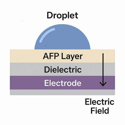
Electrowetting on dielectric is the method used to move droplets on a DMF surface. When voltage is applied to an electrode under a hydrophobic dielectric layer, it lowers the contact angle of the droplet above it, causing the droplet to spread and move. By sequentially energizing electrodes, droplets can be moved, split, merged, or mixed — all with high precision. This method works only when the surface stack (electrode, dielectric, hydrophobic topcoat) is engineered with the right materials — including AFP layers.
Why are amorphous fluoropolymers used in digital microfluidic devices?
Amorphous fluoropolymers like CyclAFlor materials provide the low surface energy, dielectric strength, and chemical resistance required for reliable electrowetting. They serve as the hydrophobic topcoat in EWOD devices, enabling consistent droplet behavior without fouling, degradation, or loss of control. Unlike PDMS, AFPs resist swelling, handle a wider temperature range, and don’t degrade under biological or chemical exposure — making them ideal for lab-on-a-chip and digital microfluidic platforms.
What applications use digital microfluidics and AFP-coated surfaces?
DMF technology is used across multiple fields, including:
- Drug discovery – to automate compound screening and reaction optimization
- Diagnostics – in lab-on-a-chip PCR and point-of-care testing platforms
- Synthetic biology – for gene editing and enzymatic assays
- Newborn screening – for high-throughput testing of metabolic disorders
- Environmental monitoring – in portable sensors for water quality or contaminants
In each of these, AFP-coated surfaces are critical to ensuring accurate, repeatable droplet control in rugged, real-world conditions.
What challenges do AFPs solve in lab-on-a-chip systems?
Lab-on-a-chip devices demand surfaces that can maintain droplet performance over thousands of cycles, resist harsh reagents, and integrate with optics and electronics. AFPs solve all three problems. They’re chemically inert, optically clear, and thermally stable — and they maintain a low surface energy even after repeated actuation. This durability and consistency make AFPs a go-to solution when devices move from the prototype phase to high-volume deployment.
Can AFP coatings be integrated into commercial digital microfluidics platforms?
Yes — and they already are. CyclAFlor films are designed for scalable integration into silicon, glass, and flexible substrates, using processes compatible with microelectronics manufacturing. Whether you’re developing disposable cartridges or high-end analytical tools, AFPs can be deposited as thin, uniform layers to meet your design and regulatory requirements. They’re ready for the real world, not just the lab bench.