Part 1 of a Two-Part Series on Optical Interposers and the Waveguide Materials That Enable Them
Breaking the Bandwidth Bottleneck
Modern computing systems — whether powering artificial intelligence, high-performance scientific research, or cloud services — are really networks of chips having nonstop conversations. CPUs pull data from memory, GPUs exchange results, and specialized accelerators stream information back and forth. The speed and efficiency of these conversations determine how well the whole system performs.
Today, most chips connect through copper traces inside silicon interposers. You can think of them as tiny highways moving electrons between processors and memory. The problem is the “wiring” that carries these signals is maxing out. For modern workloads like training an AI model or running a data center full of servers, this “traffic jam” threatens to become the limiting factor. Signals lose strength, power consumption climbs, and heat builds up.
That’s why the semiconductor industry is exploring new kinds of “express lanes” for data. Chipmakers and packaging engineers are developing better ways to keep data flowing while using less energy and generating less heat. One promising solution is the optical interposer — instead of pushing electrons through wires, the idea is to send light through tiny optical waveguides built directly into the interposer. Think of it as replacing clogged highways with high-speed rail — faster, cooler, and far more energy efficient.
What is an Optical Interposer?
If you pop open a computer chip package, you’d see the processors aren’t soldered directly to one another like wires in a lamp. They sit on a kind of middle layer called an interposer. Think of it like the foundation of a house or the hub of an airport — it connects everything together and makes sure signals get where they need to go.
A traditional interposer uses copper wiring to route electrical signals between chips — CPU to memory, GPU to accelerator, and so on. An optical interposer does the same basic job but with an extra trick — it can also route light through tiny built-in waveguides. That means it carries data both as electricity and as photons.
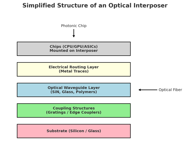 Top: Chips (CPU, GPU, ASICs) mounted directly.
Electrical routing layer: Metal traces for short-reach connections.
Optical waveguide layer: Made of SiN, glass, or polymers.
Coupling structures: Gratings or edge couplers to direct light.
Substrate: Silicon or glass foundation.
Interfaces: Photonic chip integration on top and fiber coupling at the side.
Here’s what it enables:
- Electrical lanes: Short, copper connections still handle the quick, local handshakes between chips.
- Optical express lanes: Light-based paths take over the heavy traffic, moving huge amounts of data without the heat and energy penalty.
- Couplers: These are like on-ramps and off-ramps, connecting chips inside the package or linking the waveguide layer to optical fibers that run outside the box.
Put simply, an optical interposer is the “switchboard” that makes a modern chip package work, except now it can switch both electrons and photons. That dual role is what makes it so promising as computers keep pushing for more speed.
Why Now?
A few big trends are converging to make optical interposers more than just a lab idea:
- Soaring bandwidth demand: Training AI models and running modern data centers require moving terabits of data every second. Copper wiring is struggling to keep up.
- Chiplet designs: With Moore’s Law slowing, companies are stitching systems together from many smaller chips. That only works if the “glue” between them is fast and efficient.
- Power and heat limits: Copper interconnects burn more energy per bit and generate more heat as speeds climb. Optical links can move the same data with less energy and less thermal strain.
- Manufacturing maturity: Advances in silicon photonics, glass substrates, and polymer waveguides have made large-scale optical integration technically feasible.
Put simply — the demand is here, the technology is ready, and the timing is right.
Advantages
- Headroom for growth: Light can carry much more data than copper, helping future-proof system bandwidth.
- Better energy efficiency: Lower power per bit means cooler, more efficient systems.
- Denser integration: Optics can support the high-speed, chip-to-chip links needed for multi-die packages.
Challenges to Solve
- Complex manufacturing: Aligning electronic and optical components at nanometer scales is extremely difficult.
- Material trade-offs: Silicon, glass, and polymers each bring benefits but also drawbacks. No single material solves everything.
- System integration: Electronics and optics must coexist in tight spaces with heat and reliability pressures.
The Materials Question
Optical interposers promise faster, cooler, and more efficient connections — but whether they deliver depends on one critical piece — the waveguides. These tiny channels are the “tracks” that carry light between chips. The choice of material for those tracks determines how well light is confined, how much data moves without loss, and how reliably the whole package works.
Right now, most waveguides are made from silicon, silicon nitride (SiN), or glass. They’re proven, but each comes with trade-offs in loss, fragility, or ease of integration. That’s why researchers are also looking at alternatives — including some less familiar candidates like amorphous fluoropolymers. These plastics have unusual optical properties that could make them a surprisingly good fit for the job.
Learn More
In Part 2, we’ll dig into waveguide materials — what makes a good one, how the conventional options stack up, and why fluoropolymers such as CYTOP®, Teflon AF™, and CyclAFlor® might deserve a second look as the building blocks of future optical interposers.
Frequently Asked Questions (FAQs)
What is an optical interposer in semiconductor packaging?
An optical interposer is a type of substrate that connects chips inside a package. Unlike traditional copper interposers that rely only on electrical wiring, optical interposers also include optical waveguides — tiny light-guiding channels that move data as photons. This combination enables high-bandwidth, energy-efficient chip-to-chip interconnects.
Why are optical interposers important for data centers and AI computing?
Modern workloads like artificial intelligence, cloud services, and high-performance computing demand terabits of bandwidth. Copper interconnects alone create a bottleneck, consuming too much power and generating excess heat. Optical interposers use photonics to reduce energy per bit and deliver faster, cooler, and more scalable data movement in data center computing.
How do optical interposers compare to copper interconnects?
Copper interconnects are still effective for short, local signals but face limitations in power efficiency and signal integrity as speeds scale. Optical interposers combine copper lanes with optical waveguides, giving chipmakers the ability to balance reliable electrical links with high-speed light-based interconnects.
Where will optical interposers be used first?
The earliest adoption will likely be in high-performance computing and hyperscale data centers, where the demand for high-bandwidth, energy-efficient interconnects is most urgent. Over time, optical interposers could become central to advanced packaging and heterogeneous integration across the semiconductor industry.
Are optical interposers available now or still experimental?
Some early prototypes exist through silicon photonics research and packaging R&D, but commercial deployment at scale is still emerging. Progress in waveguide materials, photonics integration, and semiconductor manufacturing will determine how quickly optical interposers move from lab to industry adoption.