Part 3 of a Series on Amorphous Fluoropolymers in the AI Value Chain
AI looks like software to most of us. Underneath, however, is an enormous physical system built on advanced semiconductors, photonic data movement, power delivery, thermal management, and high-precision manufacturing.
That physical system begins in the fab.
Before an AI accelerator can train a model, route a query, or move data across a hyperscale data center, it has to be manufactured. That manufacturing process depends on lithography – the repeated patterning of microscopic circuit features onto semiconductor wafers. Lithography is one of the defining technologies behind modern chips, and it is also one of the places where specialized materials quietly determine what is possible.
Among those specialized materials are amorphous fluoropolymers, or AFPs.
AFPs matter where advanced semiconductor manufacturing requires unusual combinations of optical clarity, low absorption, chemical resistance, low surface energy, thin-film processability, and contamination control.
Pellicles are one of the clearest examples of the need for these properties.
Pellicles and AFP films – related, but not identical
A pellicle is a lithography component with a thin transparent membrane mounted on a frame and positioned above a photomask or reticle. Its purpose is to protect the patterned mask surface from particles.
An AFP film is the material layer that may serve as the pellicle membrane, particularly in deep ultraviolet, or DUV, lithography.
In this article, “AFP film” refers to the amorphous fluoropolymer material layer. “Pellicle” refers to the protective component used in the lithography system. “AFP pellicle” refers to a pellicle whose membrane is made from an AFP film. The distinction matters because the material and the component have different jobs. The AFP film must deliver optical, chemical, mechanical, and processing performance. The pellicle must function as an integrated lithography component that protects the mask without degrading the patterning process.
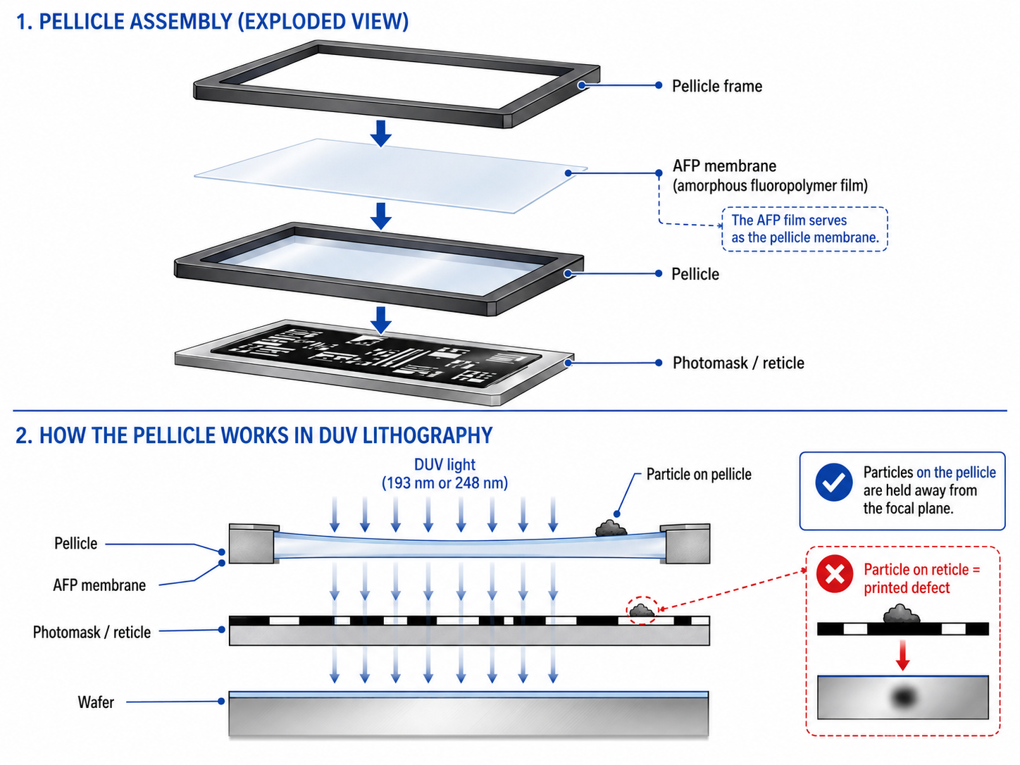
Figure 1: AFP Membrane in a DUV Pellicle Assembly
An amorphous fluoropolymer film can serve as the transparent membrane in a pellicle mounted above a photomask or reticle, keeping particles out of the focal plane during DUV lithography.
What a pellicle does
A photomask or reticle contains the pattern that will be transferred onto the wafer. It is one of the most critical and expensive components in lithography. If a contaminating particle lands directly on the mask surface, that defect can be printed repeatedly onto wafers. In high-volume semiconductor manufacturing, this can become a catastrophic yield problem.
A pellicle helps manage that risk by holding particles away from the patterned mask surface, keeping them outside the focal plane. A particle on the pellicle is less likely to print as a sharp defect on the wafer than a particle sitting directly on the reticle.
A pellicle has to protect the mask while interfering as little as possible with the lithography process. It must transmit the exposure wavelength. It must remain thin and uniform. It must avoid optical distortion. It must resist radiation and chemical degradation. It must not shed particles. It must not contaminate the mask or scanner environment. It must survive handling, mounting, inspection, cleaning protocols, and repeated exposure in demanding process conditions.
In other words, the pellicle has to be almost invisible optically while still doing a very physical job.
That is why material selection matters.
Why AFP films are useful in DUV pellicles
A useful lithography film must function as a system material. Deep ultraviolet lithography uses short-wavelength ultraviolet light, including 248 nm KrF and 193 nm ArF exposure systems. These wavelengths place significant demands on pellicle membrane materials. The film must transmit deep UV light with low absorption, maintain optical uniformity, resist degradation, and avoid introducing defects into an already unforgiving process.
Amorphous fluoropolymers are useful because they offer a rare combination of properties:
- high optical clarity that crystalline fluoropolymers generally do not provide;
- low absorption in relevant thin-film configurations;
- low refractive index that reduces optical interface effects in selected film designs;
- chemical resistance preserves performance in harsh processing environments;
- low surface energy helps reduce wetting or contamination reactions;
- solution processability enables thin, uniform films.
Many materials are optically clear but not chemically robust. Some are chemically resistant but not easily formed into high-quality transparent thin films. Others can be coated but do not have the right UV transmission, refractive index, cleanliness, or long-term stability. AFPs are specialty materials for situations where several difficult requirements have to be met at once, and DUV pellicles are exactly that kind of situation.
The pellicle is small. Its role is not.
A semiconductor fab is an exercise in controlled complexity. Hundreds of process steps must work together. Each layer must align with prior layers. Each exposure must preserve pattern fidelity. Each film, chemical, component, and surface must avoid adding contamination or variability.
In this context, it’s easy to underestimate pellicles because they are not the chip, the wafer, the scanner, or the reticle pattern itself. But if mask contamination causes defects, rework, inspection burden, tool downtime, or yield loss, the cost can be far greater than the cost of the material intended to prevent the problem. Pellicles are critical supporting components that contribute to process stability and yield protection.
That is one reason AFP films are relevant to the AI value chain. AI chips are among the most demanding semiconductor devices ever produced. The manufacturing infrastructure behind them depends on materials that preserve precision at scale.
Why DUV matters in the EUV era
Extreme ultraviolet lithography receives enormous attention because it enables the smallest and most complex features in leading-edge chips. EUV uses 13.5 nm light and can simplify patterning for certain critical layers that would otherwise require multiple DUV patterning steps.
Modern chips are built layer by layer, but not every layer needs the smallest possible feature size and justifies the cost and complexity of EUV. Many layers can still be patterned effectively and more economically with DUV lithography.
This means advanced semiconductor manufacturing often uses EUV and DUV together. EUV is used where its resolution and process simplification justify the expense; say, when one EUV exposure can replace a more complex and costly sequence of DUV exposures, etches, depositions, and alignment steps. At some point, the complexity of multi-patterning can make EUV the lower-cost total process route despite the much higher tool cost. But below that crossover point, DUV remains the better answer. If DUV can pattern the layer cleanly and economically, there is little reason to use EUV.
Why that matters for AFP pellicles
This complementary use of DUV and EUV is important for the long-term outlook for AFP films used in pellicles. If EUV were simply replacing DUV, the need for DUV pellicle materials would decline. A more realistic view is that DUV remains a durable part of advanced semiconductor manufacturing. EUV handles the most critical layers. DUV continues to handle many other layers.
As long as DUV lithography remains widely used, fabs will need DUV mask protection. As long as DUV mask protection is needed, pellicle membranes must meet demanding optical, mechanical, chemical, and contamination-control requirements. And as long as those requirements remain difficult to satisfy, AFP films will remain strategically important materials for DUV pellicle applications.
The AI value-chain connection
AI demand increases the need for advanced chips. Advanced chips depend on semiconductor fabs. Fabs depend on lithography. Lithography depends on photomasks, reticles, pellicles, optical films, contamination control, and materials that preserve pattern fidelity. AFPs matter where they help those systems work.
Conclusion: the hidden film behind the chip
AI chips begin in the fab, and fabs depend on layers of materials that most end users will never see. Pellicles are one of those layers. They protect photomasks, support yield, and help preserve the precision of lithographic patterning. In DUV lithography, AFP films can provide a valuable combination of optical transparency, chemical resistance, low refractive index, low surface energy, and thin-film processability.
They matter because advanced semiconductor manufacturing depends on specialized materials that solve specific, difficult problems. DUV pellicles are one of those problems and AFPs are one of the material families capable of addressing it.
As AI demand continues to drive investment in advanced chips, the materials behind the lithography process will remain strategically important.
The chip gets the attention.
The fab makes it possible.
And sometimes, the critical enabling material is a film so thin that its whole job is to disappear.
Learn More
If you are working on challenging applications where refractive index, interface losses, or substrate compatibility may be limiting performance, we would welcome a conversation to explore possible solutions. Contact us to learn more about our materials, capabilities, and how we can support your innovation initiatives.
References
Research papers and technical proceedings
[1] French, R. H., Gordon, J. S., Jones, D. J., Lemon, M. F., Wheland, R. C., Zhang, E., Zumsteg, F. C., Sharp, K. G., and Qiu, W. “Materials Design and Development of Fluoropolymers for Use as Pellicles in 157-nm Photolithography.” Proceedings of SPIE, Vol. 4346, Optical Microlithography XIV, 2001. DOI: https://doi.org/10.1117/12.435710
[2] French, R. H., Wheland, R. C., Qiu, W., Lemon, M. F., Zhang, E., Gordon, J., Petrov, V. A., Cherstkov, V. F., and Delaygina, N. I. “Novel Hydrofluorocarbon Polymers for Use as Pellicles in 157 nm Semiconductor Photolithography: Fundamentals of Transparency.” Journal of Fluorine Chemistry, 2003, 122, 63–80. DOI: https://doi.org/10.1016/S0022-1139(03)00081-2
[3] Lee, K., Jockusch, S., Turro, N. J., French, R. H., Wheland, R. C., Lemon, M. F., Braun, A. M., Widerschpan, T., Dixon, D. A., Li, J., Ivan, M., and Zimmerman, P. “157 nm Pellicles (Thin Films) for Photolithography: Mechanistic Investigation of the VUV and UV-C Photolysis of Fluorocarbons.” Journal of the American Chemical Society, 2005, 127, 8320–8327. DOI: https://doi.org/10.1021/ja0440654
[4] Cotte, E. P., Häßler, R., Utess, B., Antesberger, G., Kromer, F., and Teuber, S. “Pellicle Choice for 193-nm Immersion Lithography Photomasks.” Proceedings of SPIE, Vol. 5567, Photomask Technology, 2004. DOI: https://doi.org/10.1117/12.569280
[5] Zhang, H., and Weber, S. G. “Teflon AF Materials.” In Fluorous Chemistry, Topics in Current Chemistry, Vol. 308, Springer, 2012, pp. 307–337. DOI: https://doi.org/10.1007/128_2011_249
[6] Wi, S. J., Jang, Y. J., Kim, H., Cho, K., and Ahn, J. “Investigation of the Resistivity and Emissivity of a Pellicle Membrane for EUV Lithography.” Membranes, 2022, 12, 367. DOI: https://doi.org/10.3390/membranes12040367
Technical, industry, and product sources
[7] ASML, “EUV Lithography Systems.” Used for EUV wavelength, the role of EUV in printing the most intricate chip layers, and ASML’s statement that EUV and DUV systems are used in parallel.
[8] ASML, “How Microchips Are Made.” Used for general explanation of semiconductor manufacturing, chip layers, lithography, and the respective roles of EUV and DUV tools.
[9] ASML, “Indistinguishable from Magic: The EUV Pellicle.” Used for background on pellicle function and the distinct technical requirements of EUV pellicles.
[10] ZEISS, “DUV Lithography.” Used for the role of DUV lithography in semiconductor manufacturing and the continued use of DUV alongside EUV.
[11] Intel, “How a Semiconductor Factory Works.” Used for the plain-English explanation of what a fab is and how semiconductor factories operate.
[12] AGC Chemicals, “CYTOP™ Amorphous Fluoropolymers.” Used for CYTOP properties, including optical transparency, low refractive index, chemical resistance, solution processability, and pellicle-related applications.
[13] Chemours, “Teflon™ AF Resins.” Used for Teflon AF properties, including solution casting into thin films, deep-UV stability, optical clarity, and low refractive index.
[14] Chromis Technologies, “CyclAFlor® Pellicles & Coatings.” Used for CyclAFlor positioning in semiconductor pellicle films, DUV lithography, protective coatings, and optical films.
[15] U.S. Patent No. 5,061,024, “Amorphous Fluoropolymer Pellicle Films.” Used for historical support that amorphous fluoropolymer films have been disclosed for pellicle applications with high transmission in the deep ultraviolet wavelength range.
Frequently Asked Questions (FAQs)
What is a fab?
A fab, short for semiconductor fabrication plant, is the highly controlled manufacturing facility where silicon wafers are processed into integrated circuits, or chips. A fab contains cleanrooms, lithography systems, deposition tools, etch tools, inspection systems, metrology equipment, and many other process tools needed to build chips layer by layer.
What is semiconductor lithography?
Semiconductor lithography is the process used to transfer microscopic circuit patterns onto a wafer. A patterned mask or reticle defines the image, light exposes that pattern into a photoresist layer on the wafer, and subsequent processing steps use that pattern to build transistor and interconnect structures.
What is a photomask or reticle?
A photomask, often called a reticle in advanced lithography, is a precisely patterned plate that contains the circuit image to be projected onto the wafer. Because the reticle pattern is used repeatedly, contamination or defects on the reticle can create repeated defects on many chips.
What is a pellicle?
A pellicle is a thin protective membrane mounted above a photomask or reticle. Its job is to keep particles away from the mask surface. If a particle lands on the pellicle instead of the mask, it is held away from the focal plane and is less likely to print as a sharp defect on the wafer.
Is a pellicle the same thing as an AFP film?
No. A pellicle is the assembled lithography component. An AFP film is the amorphous fluoropolymer material layer that may be used as the pellicle membrane. The AFP film is the material; the pellicle is the functional component.
Why do pellicles matter?
Pellicles matter because lithography is extremely sensitive to contamination. A tiny particle on a reticle can be printed repeatedly onto wafers, creating yield loss. The pellicle acts as a contamination-control layer that helps protect the reticle and preserve pattern fidelity.
What are amorphous fluoropolymers?
Amorphous fluoropolymers, or AFPs, are specialty fluorinated polymers with a non-crystalline structure. Unlike many conventional fluoropolymers, certain AFPs can form optically clear films and can be processed from solution into thin coatings. They can combine optical clarity, low refractive index, chemical resistance, low surface energy, and thin-film processability.
Why are AFPs useful in DUV pellicles?
DUV pellicles require thin films that transmit deep ultraviolet light while maintaining uniformity, low absorption, low defectivity, chemical resistance, radiation durability, and mechanical integrity. AFPs are useful because they can provide several of these properties at the same time, which is uncommon among polymer materials.
What is DUV lithography?
DUV stands for deep ultraviolet. In semiconductor manufacturing, DUV lithography commonly refers to exposure systems using 248 nm KrF or 193 nm ArF light. DUV lithography remains a major workhorse technology in semiconductor fabs.
What is EUV lithography?
EUV stands for extreme ultraviolet. EUV lithography uses 13.5 nm light and is used for the most demanding patterning layers in leading-edge semiconductor manufacturing. EUV enables smaller features and can reduce the number of process steps needed for some highly complex patterns.
Is EUV replacing DUV?
No, not wholesale. EUV and DUV are complementary. EUV is used where its resolution and process simplification justify its cost and complexity. DUV remains the better technical and economic choice for many chip layers that do not require EUV resolution.
Why not use EUV for every layer?
EUV tools are extremely complex and expensive, and not every chip layer requires the smallest possible patterning resolution. If DUV can pattern a layer reliably and economically, there is little reason to use EUV for that layer. Fabs choose the process that gives the best balance of resolution, yield, throughput, cost, and risk.
Does the continued use of DUV matter for AFPs?
Yes. AFP films are used in DUV pellicle and lithography-film applications. Because DUV remains an important part of semiconductor manufacturing, DUV pellicle materials are not made obsolete simply because EUV adoption is growing.
Are AFPs used in EUV pellicles?
AFPs should not be casually positioned as EUV pellicle materials. EUV pellicles face a very different materials environment because 13.5 nm EUV light is strongly absorbed by most materials, and EUV pellicles must withstand high thermal and radiation loads in vacuum. DUV pellicles and EUV pellicles are related in function, but they are not the same materials problem.
What does “qualification” mean in semiconductor materials?
Qualification means proving that a material works under the actual process conditions required by the customer. For pellicle and lithography-film applications, this can include wavelength-specific transmission, absorption, film uniformity, defectivity, mechanical reliability, outgassing, contamination behavior, UV durability, chemical compatibility, and integration with the customer’s process flow.
How does this connect to AI?
AI depends on advanced chips. Advanced chips depend on semiconductor fabs. Fabs depend on lithography. Lithography depends on photomasks, reticles, pellicles, optical films, contamination control, and qualified materials. AFPs connect to the AI value chain through this upstream manufacturing role, not because they are broadly “AI materials.”
Are AFPs the answer to every lithography materials problem?
No. AFPs are valuable where their property combination matches a specific technical problem. DUV pellicles are a credible example. EUV pellicles, photoresists, hard masks, anti-reflective coatings, inspection optics, and other lithography-related systems each have their own requirements. The material fit must be proven application by application.