Part 1 of a Series on Amorphous Fluoropolymers in the AI Value Chain
Artificial intelligence is increasing demands on the physical materials, components and manufacturing systems that make high-performance computing and high-density data-center infrastructure possible. In selected components within the value chain, amorphous fluoropolymers may provide unusually valuable combinations of optical clarity, ultra-low refractive index, chemical resistance, low surface energy, and thin-film processability.
Artificial intelligence typically brings to mind large language models, training data, inference engines and the applications that increasingly affect business and daily life. This series of articles will explore its dependence on physical infrastructure – semiconductor manufacturing equipment capable of producing increasingly complex chips; advanced packaging that places logic and memory closer together; optical interconnects that move enormous volumes of data with manageable power consumption; and data centers capable of removing the heat produced by increasingly dense computing systems. This is where materials begin to matter. In later articles, we’ll explore possible roles for amorphous fluoropolymers (AFPs) in semiconductor lithography, photonic packaging and interconnects, specialty optical sensing and selected data-center monitoring applications. But first, we have to understand the physical value chain that AI demand is pulling forward.
The Upstream Effects of AI Demand
The consequences of AI demand for more training, inference, and high-performance computing (HPC) extend far upstream. AI systems require more capable accelerators, greater memory bandwidth, faster communications between processors and memory, faster communications between chips and racks, and significantly more sophisticated cooling infrastructure. A useful way to understand this value chain is to begin at its technical headwaters and follow the flow downstream:
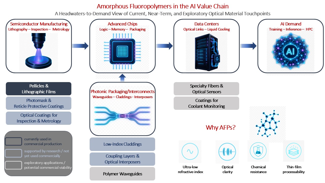
Semiconductor manufacturing and photonic packaging enable advanced chips. Advanced chips enable increasingly powerful AI/HPC data centers. Those data centers ultimately serve growing demand for AI training and inference.
The diagram attempts to simplify a value chain that is, in fact, quite complex. For example, semiconductor manufacturing and photonic packaging are integral parts of the architecture required to make advanced chips and AI systems function at scale. Likewise, cooling and monitoring become system constraints once compute density reaches the levels associated with AI accelerators. So, AI demand acts as a downstream pull on multiple upstream technologies at once.
Semiconductor Manufacturing: The Physical Starting Point
You have to make a chip before AI can run on it.
Advanced AI accelerators, graphics processing units and high-bandwidth memory devices depend on sophisticated semiconductor fabrication processes. As chip architectures become more complex and manufacturing tolerances become smaller, the requirements placed on lithography, inspection, metrology and contamination control become increasingly stringent.
Lithography is particularly important because it defines the extraordinarily fine patterns used to create semiconductor devices. Optical films and protective structures used in these environments must perform reliably under demanding conditions. They may need high optical transmission, low contamination risk, chemical resistance, dimensional stability and the ability to form very thin, uniform films.
For AFPs, this is the most immediate and technically-grounded node in the AI value chain. Semiconductor pellicles and related lithography-film applications are areas where the combination of optical clarity, chemical resistance and thin-film processability are relevant and commercially viable.
A pellicle is a thin protective membrane used to prevent particles from reaching critical patterned surfaces during semiconductor lithography. In an advanced manufacturing environment, a defect prevented upstream can have substantial benefits downstream in terms of yield, throughput, and the ability to manufacture increasingly valuable chips. While performance requirements vary by wavelength, process architecture and operating environment, semiconductor manufacturing provides a clear example of how AI demand can create upstream demand for highly specialized optical materials.
Advance Chips: More Than Shrinking Transistors
Shrinking transistor dimensions has defined semiconductor progress for decades. That remains important, but AI computing is increasingly dependent on another set of technologies – heterogeneous integration, chiplets, high-bandwidth memory and advanced packaging.
AI processors must continuously move enormous quantities of data between logic and memory. That creates what is often called the memory-bandwidth wall – the processor may be capable of performing calculations extremely quickly, but its performance is limited if data cannot be delivered to it efficiently.
High-bandwidth memory (HBM) helps address this problem by positioning memory much closer to advanced processors. Technology roadmaps cited in research [1] by Chee Ping Lee and Prahalad Parthangal describe future HBM architectures targeting bandwidths above 4 terabytes per second. These packaging architectures require very dense connections, reliable bonding materials, thermal interface materials and increasingly sophisticated substrates.
Package power is also rising rapidly. Published work [2] on AMD’s MI300X accelerator describes a package operating at approximately 750 watts, using advanced integration approaches including silicon interposers, hybrid bonding and metal thermal interface materials. Literature on thermal-management points to GPU power levels approaching 1,000 watts and AI racks approaching 100 kilowatts. [3] These figures matter because they show that the AI chip is no longer merely an electronic device. It is an integrated materials and thermal-management system.
Advanced electronic packaging may eventually require specialized dielectric materials with low electrical loss, chemical stability or compatible processing characteristics. That is a potential opportunity for AFPs, but more specific technical and commercial evidence is needed.
Photonic Packaging and Interconnects: Moving AI Data with Light
As AI systems become larger, moving data becomes as important as processing it.
Traditional electrical interconnects consume power, generate heat and face physical constraints as bandwidth density increases. This is one reason optical interconnect technologies, silicon photonics and co-packaged optics are receiving increased attention for AI and high-performance computing architectures.
Instead of relying entirely on electrical signals to move data through packages, boards and systems, photonic approaches use light for at least part of that communications task. The potential benefits include higher bandwidth, lower energy per transmitted bit and reduced signal degradation over critical distances.
An article by Yuyang Wang and colleagues provides substantial quantitative evidence that this field is advancing rapidly. Their silicon-photonics chip-I/O study reported bandwidth density above 4 terabits per second per millimeter at the shoreline of the device, with aerial density above 17 terabits per second per square millimeter and energy consumption below one picojoule per bit. [4]
These impressive numbers reveal why materials matter.
Optical signals must travel through multiple interfaces – from a photonic chip to a waveguide, from one waveguide structure to another, from an interposer to a fiber, or from a package into a larger optical network. At each transition, optical loss, alignment tolerance, refractive-index contrast and thermal stability can affect system performance.
Research has demonstrated:
- Glass substrates with integrated waveguides achieving propagation losses below 0.1 dB/cm and chip-to-waveguide coupling losses below 1 dB. [5]
- Silicon nitride-to-polymer waveguide coupling achieving losses below 1 dB at 1310 nm, with total chip-to-chip path losses below 2 dB. [6]
- Graded-index optical coupling structures designed for photonic packaging with simulated losses below 0.5 dB and broad optical bandwidth. [7]
These are the types of engineering requirements that make photonic packaging an important area for investigation of AFPs, not to replace silicon photonics platforms, glass substrates or established optical core materials, but as very-low-refractive-index claddings, selected optical coupling layers, interface materials or coatings where optical clarity, chemical resistance and processability are required together.
AI/HPC Data Centers: Power Density Changes the Cooling Problem
Eventually, advanced chips and optical interconnects are assembled into the physical systems that train and run AI models – high-performance data centers – where the effects of AI demand become particularly visible. Denser compute requires more electrical power. More electrical power produces more heat. As processor and rack power levels rise, conventional air cooling becomes increasingly difficult to use efficiently:
- The paper by Curtis, Shedd, and Clark shows GPU thermal design power approaching 700 watts, with 1,000-watt devices anticipated and AI rack power approaching 100 kilowatts. [3]
- Experimental cold-plate work has evaluated chip powers approaching 1 kilowatt and heat fluxes as high as 300 W/cm². [8]
- A controlled comparison of direct liquid cooling and air cooling for AI/ML workloads reported a 20°C reduction in chip temperature, a 12% reduction in power consumption and a 2.7% increase in throughput for the liquid-cooled system. [9]
- Google has reported scaling liquid-cooled Tensor Processing Unit infrastructure across a large AI data-center fleet, identifying coolant cleanliness and system compatibility as important reliability requirements. [10]
The research clearly shows that at high AI compute densities, liquid cooling increasingly becomes part of the enabling infrastructure.
This introduces another set of materials questions. Cooling systems may expose components to water-based coolants, glycol mixtures, dielectric fluids, corrosion-control additives and contamination risks. Monitoring systems may need to assess coolant condition, flow, contamination or degradation over long periods of operation.
Optical sensors, fiber-based sensing systems and optical flow cells could play roles in those monitoring systems. Where optical surfaces are exposed to cooling liquids, chemically resistant and low-fouling coatings may eventually be useful.
Why Consider Amorphous Fluoropolymers?
AFPs are specialty polymers distinguished by combinations of properties that can be difficult to obtain in conventional optical or protective coating materials. Depending on composition and processing approach, AFPs may offer:
- Ultra-low refractive index, potentially useful in optical cladding layers, interface management and selected coupling structures.
- High optical clarity, important for thin films and optical surfaces.
- Chemical resistance, relevant in semiconductor-processing environments and liquid-contact applications.
- Low surface energy, potentially useful where wetting, contamination or fouling must be reduced.
- Thin-film processability, important for delicate optical, patterned or microstructured surfaces.
No single property is enough to justify a new material in a demanding technical application. A very low refractive index is useful only where optical design benefits from it. Chemical resistance is valuable only if the material also meets optical, adhesion, mechanical and process requirements. A low-fouling surface is useful only if it remains stable in the actual operating fluid and environment. The opportunity for AFPs in AI infrastructure is therefore selective rather than universal. That is the premise of this series.
Our Road Map
The remaining articles in this series will move from broad value-chain context to individual technical applications. The topics we’ll explore include:
- Critical properties in optical and process-intensive AI infrastructure applications.
- Semiconductor pellicles and lithography-related films.
- Protective coatings for photomasks, inspection and metrology.
- Low-index claddings and coupling layers for photonic packaging and optical interconnects.
- Specialty fibers and optical sensing in AI/HPC environments.
- Liquid-cooling monitoring systems and the exploratory case for low-fouling optical coatings.
- A concluding framework for distinguishing credible near-term opportunities from longer-term development hypotheses.
The objective is to identify where AI infrastructure is creating difficult, valuable technical problems, and where AFPs may merit serious evaluation as part of the solution.
Conclusion
You may perceive artificial intelligence solely as a digital technology, but its expansion depends on a deeply physical value chain.
Advanced semiconductor manufacturing must produce increasingly capable processors and memory devices. Advanced packaging must bring logic, memory and communications closer together while managing enormous power densities. Photonic technologies must move data with lower energy and higher bandwidth. Data centers must cool and monitor systems whose thermal loads are rising dramatically.
Each of these developments creates materials requirements.
Some are already relevant to AFPs, particularly in specialized optical films associated with semiconductor manufacturing. Others are technically plausible adjacencies, such as low-index optical layers in photonic packaging. Still others, including surface coatings for liquid-cooling monitoring, remain exploratory appications requiring careful testing and qualification.
AI is software, but also optics, packaging, cooling, surfaces, thin films and materials engineering. In selected places along that value chain, materials with uncommon combinations of properties may prove critically important.
Learn More
If you are working on challenging applications where refractive index, interface losses, or substrate compatibility may be limiting performance, we would welcome a conversation to explore possible solutions. Contact us to learn more about our materials, capabilities, and how we can support your innovation initiatives.
References
- Lee, C. P.; Parthangal, P. Advanced Packaging Road Map to 2030: Integrating Memory, Logic, and Systems for Artificial Intelligence. IEEE Electron Devices Magazine, 2025/2026. DOI: 10.1109/MED.2026.3651987.
- Mandalapu, C. et al. 3.5D Advanced Packaging Enabling Heterogenous Integration of HPC and AI Accelerators. ECTC, 2024. DOI: 10.1109/ECTC51529.2024.00391.
- Curtis, R.; Shedd, T.; Clark, E. B. Performance Comparison of Five Data Center Server Thermal Management Technologies. SEMI-THERM, 2023. DOI: 10.23919/SEMI-THERM59981.2023.10267908.
- Wang, Y. et al. Co-Designed Silicon Photonics Chip I/O for Energy-Efficient Petascale Connectivity. IEEE Transactions on Components, Packaging and Manufacturing Technology, 2025. DOI: 10.1109/TCPMT.2024.3492189.
- Brusberg, L. et al. Glass Platform for Co-Packaged Optics. IEEE Journal of Selected Topics in Quantum Electronics, 2023. DOI: 10.1109/JSTQE.2023.3247245.
- Van Asch, J. et al. Sub-1 dB Loss SiN-to-Polymer Waveguide Coupling: An Enabler for Co-Packaged Optics. OFC, 2024. DOI: 10.1364/OFC.2024.Th2A.27.
- Weninger, D. et al. Novel Optical Bumps Using Graded Index Couplers for Flip-Chip Photonic Packaging. 2025. DOI: 10.4071/001c.147093.
- Kulkarni, D. et al. Thermal Performance of Common Cold Plate for Pumped Single- and Two-Phase Direct Liquid Cooling of High-Performance Processors. ASME IPACK, 2024. DOI: 10.1115/IPACK2024-141367.
- Ramakrishnan, B. et al. Understanding the Impact of Data Center Liquid Cooling on Energy and Performance for AI/ML Workloads. Journal of Electronic Packaging, 2024. DOI: 10.1115/1.4067136.
- Iyengar, M.; Padilla, J. Scaling Liquid Cooling for Google Data Center AI Applications to a 1 GW Fleet. ITherm, 2025. DOI: 10.1109/ITherm55376.2025.11235575.
Frequently Asked Questions (FAQs)
What are amorphous fluoropolymers?
Amorphous fluoropolymers, or AFPs, are specialty fluorinated polymers that lack the crystalline structure found in many conventional fluoropolymers. This amorphous structure can enable unusual combinations of properties, including high optical clarity, ultra-low refractive index, chemical resistance, low surface energy and thin-film processability. These properties make AFPs interesting for selected optical, semiconductor and advanced manufacturing applications.
Why are amorphous fluoropolymers relevant to artificial intelligence?
AI demand increases the need for physical infrastructure – advanced semiconductor manufacturing, high-performance chips, photonic packaging, optical interconnects and high-density data-center cooling. In selected parts of that AI value chain, AFPs may help address demanding optical, chemical, surface or thin-film materials requirements.
How does AI demand affect semiconductor manufacturing?
AI training and inference require increasingly powerful processors, graphics processing units, AI accelerators and high-bandwidth memory. These devices depend on sophisticated semiconductor fabrication, including lithography, inspection, metrology and contamination control. As chip architectures become more complex, the materials used in semiconductor manufacturing must meet increasingly demanding requirements for optical performance, chemical resistance, cleanliness and process stability.
Where are AFPs most relevant in semiconductor manufacturing?
AFPs currently are used in specialized optical films, including semiconductor pellicles and lithography-related films. Pellicles help protect critical patterned surfaces from particles during lithography. AFPs may be useful where thin, optically clear, chemically resistant films are required. The specific fit depends on wavelength, process conditions, film performance, contamination control and qualification requirements.
What is a semiconductor pellicle?
A semiconductor pellicle is a thin protective membrane used in lithography to prevent particles from reaching a photomask or reticle. By keeping particles away from critical patterned surfaces, a pellicle can help reduce defects and improve semiconductor manufacturing yield. Because pellicles are used in demanding optical environments, their materials must be carefully selected and qualified.
What is photonic packaging?
Photonic packaging refers to the integration of optical components, waveguides, fibers, interposers and related structures into electronic or optoelectronic systems. In AI and high-performance computing, photonic packaging is important because optical interconnects may help move large volumes of data with lower energy consumption and higher bandwidth than conventional electrical interconnects alone.
Why do optical interconnects matter for AI infrastructure?
AI systems must move enormous amounts of data between processors, memory, chips, servers and racks. Electrical interconnects can face limits related to bandwidth density, power consumption, heat and signal integrity. Optical interconnects use light to transmit data and may help address these limitations in AI/HPC systems, especially as compute clusters become larger and more power-intensive.
How could AFPs be used in photonic packaging and optical interconnects?
AFPs may be relevant as low-refractive-index claddings, optical coupling layers, interface materials or selected thin-film coatings. Their ultra-low refractive index may help manage optical confinement or mode-field transitions in certain designs. Their optical clarity, chemical resistance and processability may also be useful where materials must perform reliably near delicate optical interfaces. AFPs should be viewed as complementary materials, not replacements for silicon photonics, glass substrates or established optical core materials.
What does “ultra-low refractive index” mean, and why does it matter?
Refractive index describes how strongly a material bends or slows light. An ultra-low-refractive-index material can be useful in optical systems where designers need strong refractive-index contrast, low-reflection interfaces, cladding layers or controlled light confinement. In photonic packaging, low-index materials may help manage how light moves through waveguides, coupling structures and optical interfaces.
Why does AI increase demand for liquid cooling in data centers?
AI accelerators and high-performance computing systems consume large amounts of power and generate substantial heat. As chip and rack power densities rise, conventional air cooling becomes less effective or less efficient. Liquid cooling can remove heat more effectively from dense AI computing systems, which is why it is becoming increasingly important in AI/HPC data centers.
Could AFPs be used in AI data-center cooling systems?
Possibly, but this is an exploratory area. AFPs may be relevant where optical sensors, flow cells or monitoring surfaces are exposed to coolants and require chemical resistance, low fouling, optical clarity or stable surface properties. However, AFP use in coolant-monitoring systems would require application-specific testing for adhesion, optical transmission, fluid compatibility, fouling resistance and long-term reliability.
Are AFPs already widely used in the AI value chain?
No. AI infrastructure creates selected materials challenges where AFP properties may be relevant. Some opportunities, such as semiconductor pellicles and lithography-related films, are proven. Others, such as photonic packaging layers or coolant-monitoring coatings, are emerging or exploratory.
What properties make AFPs interesting for AI infrastructure applications?
The most relevant AFP properties include ultra-low refractive index, optical clarity, chemical resistance, low surface energy and thin-film processability. These properties may be valuable in optical films, semiconductor manufacturing environments, photonic packaging interfaces, specialty fibers, optical sensors and selected monitoring applications. The value depends on whether the application requires more than one of these properties at the same time.
Why is the AI value chain a materials problem?
AI may appear to be a software-driven technology, but it depends on physical systems – semiconductor fabrication, advanced chips, high-bandwidth memory, photonic packaging, optical interconnects, data-center cooling and monitoring infrastructure. Each part of this value chain imposes materials requirements. These include optical transmission, refractive-index control, thermal stability, chemical resistance, contamination control, low fouling and manufacturability.
What will later articles in this series cover?
Later articles will examine specific AI infrastructure touchpoints in more detail, including AFP properties, semiconductor pellicles, photomask and reticle protective coatings, inspection and metrology coatings, low-index claddings, optical coupling layers, photonic packaging, specialty optical sensors, and coatings for liquid-cooling monitoring systems. The goal is to distinguish credible near-term opportunities from longer-term development hypotheses.