Part 2 of a Series on Amorphous Fluoropolymers in the AI Value Chain
The first article in this series introduced the physical infrastructure behind artificial intelligence, illustrating how AI/HPC data centers create upstream demand for semiconductor manufacturing, photonic packaging, advanced chips, optical interconnects, and cooling systems. This infrastructure creates difficult physical materials problems, some of which may align with amorphous fluoropolymer (“AFP”) properties:
- ultra-low refractive index
- optical clarity
- chemical resistance
- low surface energy
- low dielectric constant
- thin-film processability.
AFPs are candidates for selected high-value interfaces, films, coatings, claddings, and surfaces where conventional materials may struggle to satisfy multiple constraints simultaneously. The strongest case for AFPs arises where an application requires several of their unique properties at the same time.
Property Combinations Matter More Than Any One Alone
Material selection in advanced technology systems typically seeks to optimize performance within a set of constraints.
An optical designer may want low refractive index, but only if the material has acceptable absorption, adhesion, and thermal stability. A semiconductor engineer may want chemical resistance, but not if the material sheds particles, contaminates the process environment, or cannot make a uniform coating. Low dielectric loss may be attractive to a packaging engineer, but the material will also have to survive integration, bonding, cleaning, and reliability testing.
The practical question is whether the material offers the right combination of properties for a specific system. The unique properties of AFPs can be useful in optics, photonics, semiconductors, sensors, surface engineering, microfluidics, and other demanding applications. In the AI value chain, the most relevant touchpoints are the optical and physical infrastructure that makes AI computing possible.
Ultra-low Refractive Index – Useful Where Optical Design Needs It
Refractive index describes how strongly a material slows and bends light. In optical systems, refractive index determines reflection, refraction, confinement, coupling, and mode behavior.
AFPs are notable because they offer some of the lowest refractive indices available among polymer materials. Depending on composition, AFP refractive index values may fall in the approximate range of 1.29 to 1.34, which is significantly lower than many conventional optical polymers and glasses. That makes AFPs interesting for applications such as low-index claddings, optical coatings, anti-reflective interfaces, and selected coupling structures.
In the AI infrastructure context, this matters most in photonic packaging and optical interconnects.
As AI systems scale, moving data becomes a major power and performance challenge. Optical interconnects, silicon photonics, co-packaged optics, optical interposers, and waveguide-based routing are all being explored to increase bandwidth and reduce energy per bit. These systems often require optical signals to pass through multiple interfaces – chip to waveguide, waveguide to interposer, interposer to fiber, or package to network. At each transition, refractive index can affect optical loss, mode-field mismatch, confinement, and coupling efficiency.
AFPs may be useful where a very-low-index material is needed to serve as a cladding, interface layer, optical buffer, or coupling aid. While they have low refractive index, however, this is not inherently valuable unless they can also satisfy other integration requirements of a specific photonic package, waveguide structure, or optical interface.
Optical Clarity – Transmission Is Necessary, But Not Sufficient
AFPs are also known for high optical clarity, with transparency across broad wavelength ranges, including ultraviolet, visible, and near-infrared regions, depending on composition, thickness, and processing. That matters because AI infrastructure depends heavily on optical systems:
- Semiconductor lithography uses light to pattern chips.
- Inspection and metrology systems use optical methods to detect defects and measure structures.
- Photonic packaging uses light to move data within or between systems.
- Optical sensors may be used in data-center monitoring, cooling systems, or specialty infrastructure.
- Optical fibers and waveguide interfaces increasingly support high-bandwidth computing environments.
In these applications, optical clarity is a threshold property. A material that absorbs, scatters, yellows, hazes, or degrades under exposure conditions may not be usable, no matter how attractive its other properties are.
For semiconductor pellicles and lithography-related films, optical transmission and uniformity are critical. A pellicle or protective optical film must transmit the relevant wavelength while minimizing distortion, contamination risk, and degradation. In photonic packaging, optical films and claddings must avoid adding unacceptable propagation or coupling loss. In optical sensing applications, the windows, coatings, or flow-cell interfaces must remain clear over time in real-world operating environments.
So while optical clarity may warrant a material’s consideration, it does not mean it will get qualified. The material must retain optical performance after coating, drying, curing, thermal exposure, chemical exposure, cleaning, handling, and long-term aging. That is where lifecycle evidence becomes essential.
Chemical Resistance – Valuable in Harsh Processing and Operating Environments
Chemical resistance is one of the classic strengths of fluorinated materials. AFPs provide resistance to solvents, acids, bases, moisture, oils, and other aggressive environments, depending on the polymer structure and use conditions. In the AI value chain, chemical resistance is relevant in at least three areas.
First, semiconductor manufacturing uses demanding process environments. Lithography, etching, cleaning, deposition, inspection, and metrology all impose strict requirements on materials that may contact chemicals, vapors, particles, radiation, or sensitive surfaces. Any material used in these environments must be evaluated not only for chemical resistance, but also for contamination control, outgassing, particle generation, extractables, and compatibility with process flows.
Second, photonic packaging and optical interconnects may involve multiple materials and process steps – substrates, waveguides, claddings, adhesives, coatings, solder reflow, bonding, cleaning, and environmental exposure. A material used near optical interfaces must remain stable through integration and operation. Chemical resistance can be valuable, but only if the material also adheres, coats uniformly, maintains optical properties, and avoids reliability problems.
Third, AI/HPC data-center cooling introduces liquid-contact environments. Direct liquid cooling and immersion cooling can expose materials to water-based coolants, glycols, dielectric fluids, corrosion inhibitors, biological control additives, and particles. If optical sensors, flow cells, or monitoring windows are placed in those environments, their surfaces must resist fouling, chemical attack, swelling, clouding, or index changes. Coolant chemistry, exposure time, temperature, flow conditions, and cleaning methods can all affect performance. While this is a plausible future area for AFPs, lifecycle evidence is scant and it should be treated as exploratory unless supported by application-specific testing.
Low Surface Energy – Useful When Wetting, Fouling, or Contamination Matters
Low surface energy is another important AFP property. It can reduce wetting by water, oils, or other liquids, and it can influence adhesion, contamination, fouling, and cleanability.
This property has obvious relevance in surface engineering. It is one reason fluorinated coatings are used in applications where repellency, anti-fouling behavior, or controlled wetting are valuable. But low surface energy has tradeoffs. A surface that resists wetting may also resist adhesion. A coating that repels contamination may be harder to bond to a substrate. A low-fouling surface still has to survive mechanical handling, abrasion, chemical exposure, and long-term use.
In the AI infrastructure context, low surface energy may be relevant in:
- Semiconductor environments where contamination control is important.
- Optical inspection or metrology surfaces where cleanability matters.
- Microfluidic or coolant-monitoring systems where fouling or wetting behavior may affect sensor performance.
- Optical windows, flow cells, or sensor surfaces exposed to liquids.
- Protective coatings where surface cleanliness and chemical resistance must be combined.
The value of low surface energy depends on the failure mode. If the real problem is particle contamination, residue formation, wetting instability, or fouling, then surface properties may matter. If the real problem is mechanical strength, thermal expansion, or electrical breakdown, low surface energy may be secondary or irrelevant.
Again, the material property has to match the system problem.
Thin-film Processability – The Bridge From Property to Part
A material can have ideal laboratory properties and still be useless if it can’t be implemented commercially.
Thin-film processability is central to the AFP value proposition. AFPs that are soluble in suitable fluorinated solvents can be coated by methods such as spin coating, dip coating, spray coating, or other solution-based deposition methods. This can allow thin, uniform films to be formed on substrates, optical surfaces, patterned structures, or delicate components.
For AI infrastructure applications, thin-film processability may matter in:
- Semiconductor pellicles and lithography-related films.
- Protective optical coatings.
- Low-index cladding layers.
- Optical coupling or interface layers.
- Waveguide-adjacent structures.
- Sensors, flow cells, and optical monitoring surfaces.
- Conformal coatings for delicate components.
Processability is where materials science meets manufacturing reality. A thin film must have the right thickness, uniformity, roughness, adhesion, defect density, drying behavior, and long-term stability. It must also be compatible with the customer’s process window.
For many advanced applications, the film is the product. A polymer pellet or powder is not enough. The material has to become a controlled surface, membrane, coating, or interface.
This is one reason AFPs can be interesting. Their value may lie less in bulk material properties and more in the ability to create specialized thin films with combinations of optical, chemical, and surface performance.
Low Dielectric Constant – A Watchlist Property for Advanced Packaging
AI chips are increasingly integrated systems, with advanced packaging bringing logic, memory, power delivery, interconnects, and thermal-management structures closer together. As signal speeds rise and package architectures become more complex, dielectric materials can influence electrical performance, signal loss, cross-talk, thermal behavior, and reliability.
AFPs may offer low dielectric constant and strong electrical insulation, which makes them interesting as potential materials for selected electronic or photonic packaging applications. Low dielectric constant materials are often valuable where signal propagation, high-frequency performance, or electrical isolation matter.
That said, advanced electronic packaging is unforgiving. A material must satisfy integration, mechanical, thermal, adhesion, coefficient-of-thermal-expansion, moisture, reliability –and fit into established manufacturability process flows and cost structures – in addition to having an attractive dielectric constant.
AFPs may eventually have a role in selected low-loss dielectric or insulating applications, particularly where optical and chemical properties are also useful, but this is not yet the strongest or most immediate AI value-chain opportunity compared with semiconductor optical films or photonic cladding and coupling layers. This AFP opportunity should remain on the watchlist for now.
Thermal and Environmental Stability – Surviving Real Use Conditions
AI infrastructure increasingly combines optical, electrical, thermal, and chemical stress.
Semiconductor manufacturing environments can involve radiation, heat, chemicals, and contamination sensitivity. Photonic packaging places optical interfaces near heat-generating chips and mechanically complex assemblies. Data-center cooling systems expose materials to liquids, additives, temperature cycling, and long operating times.
A material that performs well in the lab may still fail after real-world exposure to:
- Elevated temperature.
- UV radiation or optical power.
- Cleaning chemicals.
- Process solvents.
- Humidity or moisture.
- Coolants or dielectric fluids.
- Thermal cycling.
- Mechanical stress.
- Long-term aging.
- Contamination-sensitive environments.
This is where the distinction between material potential and system readiness becomes important. AFPs may offer useful thermal, chemical, optical, and surface properties, but each application still requires lifecycle evidence. That evidence may include optical transmission over time, film adhesion, outgassing, contamination testing, thermal aging, chemical soak testing, dimensional stability, coating uniformity, and performance under actual operating conditions.
A material becomes an AI infrastructure solution only when it generates enough lifecycle evidence to justify integration.
Matching AFP Properties to AI Infrastructure Problems
The most useful way to think about AFPs in the AI value chain is as a matching exercise.
The relevant questions are:
- What is the system problem?
- Which material property is limiting performance?
- Does the application require a combination of properties?
- Can AFPs provide that combination?
- Can the material be processed into the required form?
- Can it survive the integration environment?
- Can it generate enough lifecycle evidence to justify adoption?
- Do the economics support the business case?
Using that framework, the strongest AI-infrastructure opportunities for AFPs fall into several categories.
Semiconductor Optical Films and Pellicles
This is the most immediate and technically grounded category. The need for optical clarity, thin-film uniformity, chemical resistance, and contamination control aligns well with the AFP property set. Specific applications still depend on wavelength, mechanical requirements, process compatibility, and qualification standards.
Photomask, Reticle, Inspection, and Metrology Coatings
These are logical adjacencies to lithography-related films. Optical surfaces in semiconductor manufacturing environments may benefit from coatings that combine transmission, chemical resistance, cleanability, and thin-film processability. These opportunities require careful evaluation because coating defects, haze, particles, adhesion failure, or contamination can quickly eliminate a candidate material.
Photonic Packaging Claddings and Coupling Layers
This is one of the most interesting emerging areas. Low refractive index, optical clarity, and thin-film processability may be useful in claddings, optical coupling layers, mode-field management structures, or interposer-related interfaces. AFPs should be viewed as complementary materials in this context, not as replacements for silicon photonics, glass, silicon nitride, or established optical core materials.
Specialty Optical Sensors and Fibers
AFPs may be useful where optical clarity, low index, chemical resistance, or surface behavior matters in specialty fibers, sensing structures, or optical monitoring systems, but require targeted testing to confirm their value.
Cooling-system Monitoring Surfaces
This use case remains exploratory. AI/HPC data-center liquid cooling creates possible needs for durable monitoring systems, including optical sensors and flow cells. AFP coatings may be relevant where optical surfaces must resist fouling, chemical attack, or wetting instability in coolant-contact environments, but this opportunity requires more evidence before strong claims can be made.
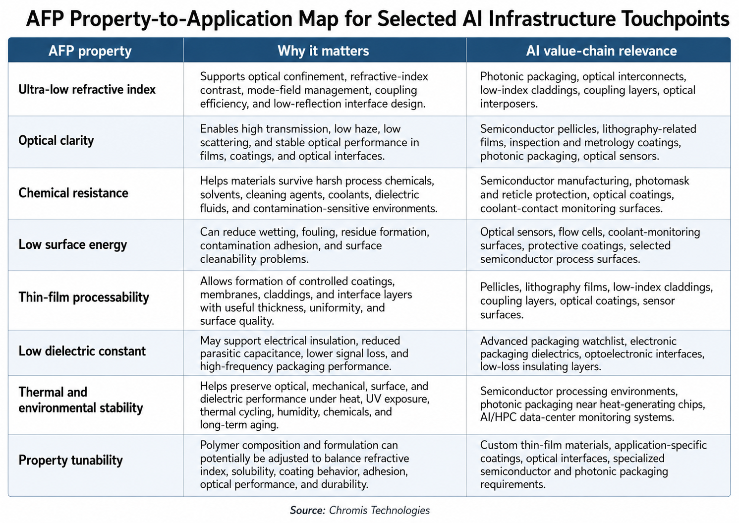
The table below summarizes how key AFP properties align with selected AI infrastructure requirements, though they may not be qualified for every listed application. Rather, the table serves as a screening framework for identifying where AFPs may merit serious consideration.
Where AFPs Do Not Automatically Win
It’s important to understand the limits of AFPs. Despite their intriguing properties, they may not work because:
- The lowest refractive index is not always the optimal refractive index.
- Chemical resistance does not solve poor adhesion.
- Low surface energy can complicate bonding and integration.
- Optical clarity at one wavelength does not guarantee performance at another.
- Thin-film coating in the lab does not guarantee manufacturability.
- A promising property combination does not eliminate cost pressure.
- Qualification timelines in semiconductor and photonic systems can be long.
- Incumbent materials may be good enough, cheaper, or already qualified.
The “good enough” problem is real. A material can work beautifully and still lose if the system only needs a cheaper material that performs adequately. For AFPs, the best opportunities are likely to be applications where the property combination is difficult to obtain elsewhere, the system problem is expensive or limiting, and the customer has a reason to evaluate a specialized material.
The Qualification Mindset
In the AI infrastructure value chain, materials innovation becomes valuable only when it supports a real integration decision. For AFPs, that means moving from property claims to lifecycle evidence. Depending on the application, that evidence may include:
- Refractive index at the relevant wavelength.
- Optical transmission through the actual film thickness.
- Absorption, haze, and scattering.
- Film thickness uniformity.
- Surface roughness.
- Adhesion to the actual substrate.
- Thermal aging.
- UV or optical-power exposure.
- Chemical soak testing.
- Coolant compatibility.
- Outgassing and extractables.
- Particle generation.
- Dielectric performance.
- Mechanical durability.
- Process repeatability.
- Long-term performance stability.
- Cost and supply-chain viability.
This does not mean every opportunity requires the same testing. For example, a pellicle film, optical cladding, coolant-monitoring coating, and electronic packaging dielectric each have different qualification paths. But the underlying principle is the same – properties must become evidence.
Conclusion
AI infrastructure is creating a new set of materials challenges, but not every advanced material belongs in the AI value chain.
AFPs are interesting because they combine properties that are often difficult to obtain together – ultra-low refractive index, optical clarity, chemical resistance, low surface energy, low dielectric constant, and thin-film processability. That combination may matter in selected optical films, claddings, coupling layers, protective coatings, sensors, and monitoring surfaces. But the opportunity is selective. AFPs will matter only where their property set maps to a specific system problem, where they can be processed into the required form, where they can survive the real integration environment, and where the business case supports adoption.
That is the framework for the rest of this series.
In the next article, we will examine the most immediate and technically grounded opportunity for AFPs in the AI value chain – semiconductor pellicles and lithography-related films.
Learn More
If you are working on challenging applications where refractive index, interface losses, or substrate compatibility may be limiting performance, we would welcome a conversation to explore possible solutions. Contact us to learn more about our materials, capabilities, and how we can support your innovation initiatives.
References
- Lee, C. P.; Parthangal, P. Advanced Packaging Road Map to 2030: Integrating Memory, Logic, and Systems for Artificial Intelligence. IEEE Electron Devices Magazine, 2025/2026. DOI: 10.1109/MED.2026.3651987.
- Wang, Y. et al. Co-Designed Silicon Photonics Chip I/O for Energy-Efficient Petascale Connectivity. IEEE Transactions on Components, Packaging and Manufacturing Technology, 2025. DOI: 10.1109/TCPMT.2024.3492189.
- Van Asch, J. et al. Sub-1 dB Loss SiN-to-Polymer Waveguide Coupling: An Enabler for Co-Packaged Optics. OFC, 2024. DOI: 10.1364/OFC.2024.Th2A.27.
- Zhao, Y.; Hu, F.; Tenhaeff, W. E. “Control of Fluoropolymer Crystallinity for Flexible, Transparent Optical Thin Films with Low Refractive Indexes.” Macromolecules 2025, 58(3), 1265–1278. https://doi.org/10.1021/acs.macromol.4c02242 (pubs.acs.org).
Frequently Asked Questions (FAQs)
What are the most important AFP properties for AI infrastructure?
The most relevant AFP properties are ultra-low refractive index, optical clarity, chemical resistance, low surface energy, low dielectric constant, and thin-film processability. These properties may be useful in selected semiconductor, photonic packaging, optical sensing, and data-center monitoring applications.
Why does refractive index matter in photonic packaging?
Refractive index affects how light is confined, guided, coupled, and reflected at optical interfaces. In photonic packaging and optical interconnects, low-refractive-index materials may be useful as claddings, coupling layers, optical buffers, or interface materials where optical loss and mode-field behavior are important.
Are AFPs useful only because they have low refractive index?
No. Low refractive index is important, but AFPs are most interesting where several properties are needed together. For example, a photonic packaging layer may require low index, optical transparency, thin-film uniformity, thermal stability, and process compatibility. A semiconductor coating may require optical clarity, chemical resistance, cleanliness, and low defectivity.
How does optical clarity affect AFP applications?
Optical clarity is essential for applications involving lithography, optical films, waveguides, sensors, inspection systems, and photonic packaging. A material must transmit the relevant wavelength with acceptable absorption, haze, scattering, and stability over time.
Why is chemical resistance important in AI infrastructure?
AI infrastructure depends on semiconductor manufacturing, advanced packaging, photonics, and high-density data centers. These environments may expose materials to chemicals, solvents, cleaning agents, coolants, moisture, thermal cycling, or contamination-sensitive processes. Chemical resistance can be valuable when combined with optical and processing performance.
What does low surface energy mean?
Low surface energy means a surface is less easily wetted by liquids such as water or oils. This property can support repellency, cleanability, anti-fouling behavior, or controlled surface interactions. In AFPs, low surface energy may be useful for coatings, optical surfaces, sensing interfaces, and liquid-contact applications.
Why is thin-film processability important?
Many AFP opportunities involve coatings, membranes, claddings, or optical interface layers rather than bulk parts. Thin-film processability allows AFPs to be applied as controlled films on substrates or components. The resulting film must meet requirements for thickness, uniformity, adhesion, optical transmission, roughness, and stability.
Could AFPs be used as low-dielectric materials in advanced packaging?
Possibly, but this should be treated as a watchlist opportunity. AFPs may offer low dielectric constant and strong electrical insulation, but advanced packaging applications require extensive evidence for integration compatibility, adhesion, reliability, thermal performance, manufacturability, and cost.
What makes AFPs different from conventional fluoropolymers?
Unlike many crystalline or semicrystalline fluoropolymers, AFPs are amorphous. This can provide high optical clarity, solution processability, low refractive index, chemical resistance, and useful surface properties. Those differences can make AFPs suitable for optical films, coatings, claddings, and selected high-performance thin-film applications.
Where are AFPs most likely to matter in the AI value chain?
The strongest current opportunity is in semiconductor optical films, including pellicles and lithography-related films. Emerging opportunities include photomask and reticle protective coatings, inspection and metrology coatings, low-index claddings, coupling layers, and selected photonic packaging interfaces. More exploratory opportunities include optical sensors and coatings for liquid-cooling monitoring systems.
Are AFPs already used broadly in AI systems?
No. AFPs should not be described as broadly used AI materials. The better framing is that AI infrastructure creates selected materials challenges where AFP properties may be relevant. Each potential application requires specific technical evidence, qualification, and economic justification.
What does “lifecycle evidence” mean for AFP applications?
Lifecycle evidence means data showing that a material can perform reliably over the life of the application. For AFPs, this may include optical transmission over time, refractive-index stability, adhesion, thermal aging, UV exposure, chemical resistance, coolant compatibility, contamination control, outgassing, particle testing, and process repeatability.
What will the next article in this series cover?
The next article will focus on semiconductor pellicles and lithography-related films, which represent one of the most immediate and technically grounded areas where AFPs may support the AI value chain.