

The 7th and final article in our Series on Amorphous Fluoropolymers in the AI Value Chain
Throughout this series, we have focused on the materials that enable AI infrastructure to be manufactured, packaged, connected, cooled and monitored. Amorphous fluoropolymers, or AFPs, are interesting where their unusual combination of properties — ultra-low refractive index, optical clarity, chemical resistance, low surface energy, low dielectric constant and thin-film processability — maps to a real infrastructure problem.
We’ve examined available evidence to determine where these properties matter at various touchpoints along the AI value chain, while recognizing that commercial proof requires viable economics and not just technical performance.
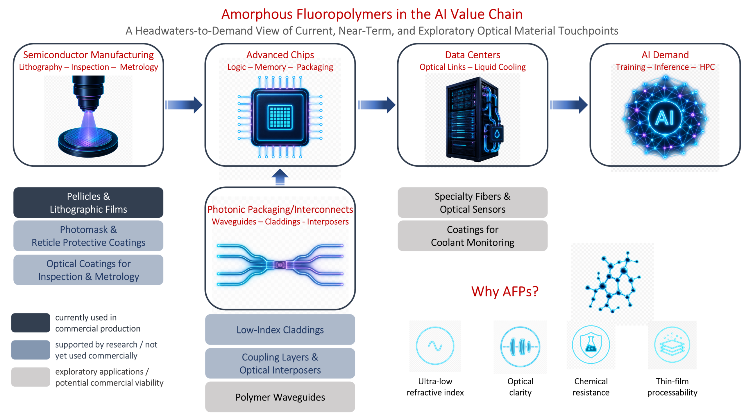
Figure 1. AFP touchpoints in the AI value chain. Semiconductor manufacturing and photonic packaging enable advanced chips, which support AI/HPC data centers and ultimately serve AI demand. The strongest AFP opportunities are in semiconductor optical films and lithography-related applications, while photonic packaging, optical sensing and coolant-monitoring applications remain emerging or exploratory.
The diagram above, first introduced at the start of this series, summarizes the AI value-chain framework we have been using. Semiconductor manufacturing and photonic packaging enable advanced chips. Advanced chips enable AI/HPC data centers. Those data centers ultimately support the growing demand for AI training and inference. [1]
In this concluding article, we return to that framework to map where AFP applications are already established, where they appear most technically grounded, where they remain emerging, and where they should still be treated as exploratory.
AI infrastructure creates materials problems
The first article in this series began with the simple premise that in addition to software, AI depends on a physical value chain extending upstream into semiconductor manufacturing and downstream into data-center infrastructure. [1]
Each step in that value chain creates materials requirements. Semiconductor manufacturing requires lithography, inspection, metrology and contamination control. Photonic packaging and optical interconnects require low-loss optical interfaces, waveguides, claddings, coupling layers and interposers. AI/HPC data centers require high-density cooling, monitoring, optical links and reliable sensing infrastructure. [7, 8, 9, 13]
Those systems increasingly combine optical, chemical, thermal, electrical and surface-performance demands, elevating the importance of specialty materials.
Why AFPs were worth examining
The second article in this series made the case that AFPs are most attractive when the application requires a difficult combination of their unique properties.
A low-index optical cladding, for example, may also need high transparency, low haze, thermal stability, coating uniformity and compatibility with nearby materials – requirements that published fluoropolymer thin-film research continues to explore. [17]
. A lithography-related optical film may need transmission, chemical resistance, low defectivity and contamination control. A coolant-monitoring surface may need optical clarity, low fouling, chemical compatibility and long-term stability in the actual fluid environment.
These combinations are the recurring theme of our series.
Where the case for AFPs appears strongest — and where evidence is still developing
The rankings on this AFP opportunity map reflect the combination of property fit, evidence maturity, and apparent distance from practical qualification at this time.
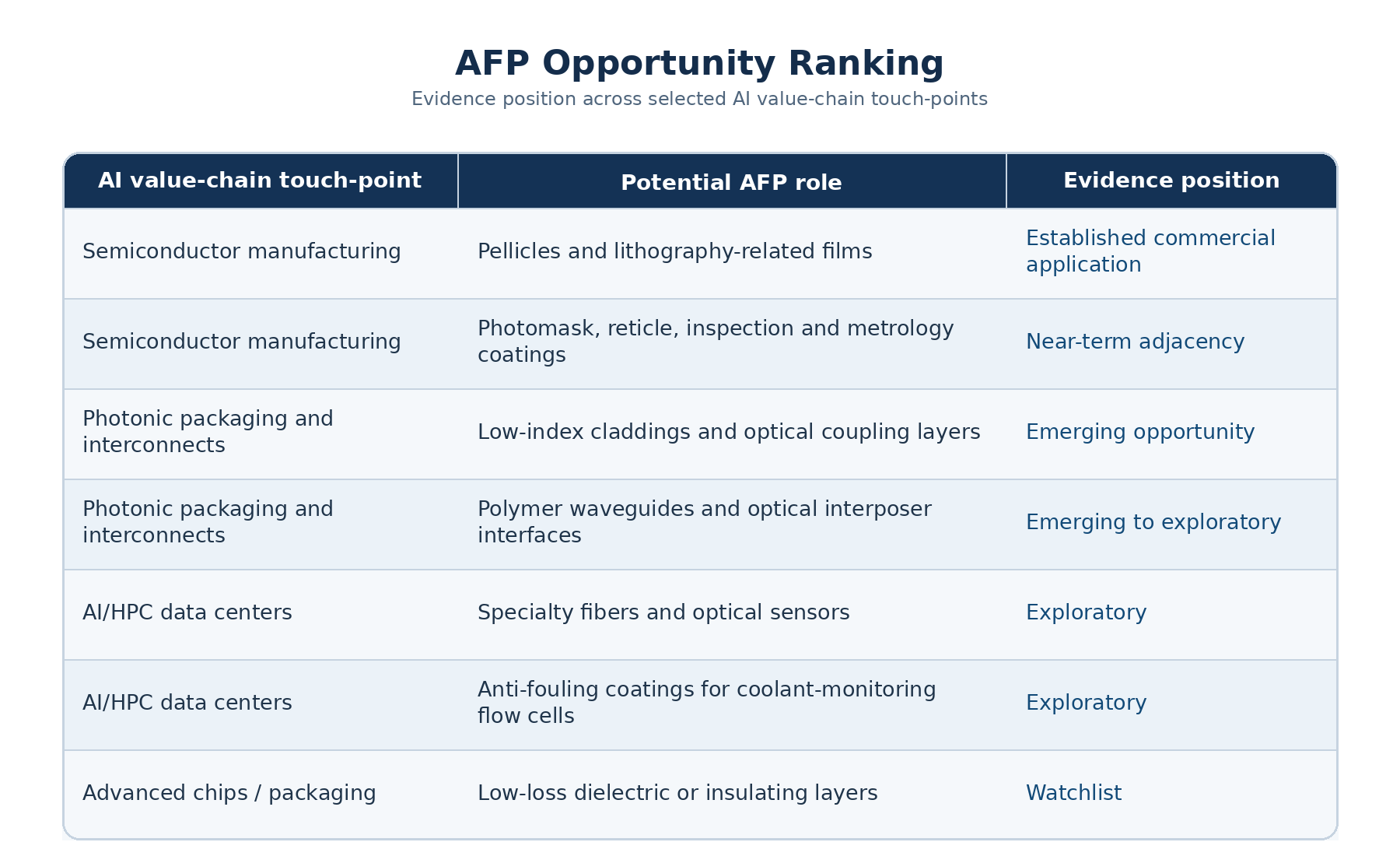
The clearest and most established AFP application in this value chain is in semiconductor manufacturing, especially pellicle films and related lithography optical films. AFPs such as CYTOP®, Teflon™ AF and CyclAFlor® Clear are already used in commercial pellicle-film production, making this an established application rather than merely a future opportunity. [2, 3, 4, 5, 6, 12]
From there, the opportunity map becomes less mature. Photomask, reticle, inspection and metrology coatings rank as near-term adjacencies because they share similar requirements — optical clarity, thin-film uniformity, chemical resistance, cleanability and low contamination risk — but have less direct proof and still require application-specific qualification.
Low-index claddings and optical coupling layers in photonic packaging rank as emerging because the need is real and the property fit is strong. Advanced packaging, silicon photonics, co-packaged optics and low-loss optical coupling all point to the importance of materials at optical interfaces, but commercial AFP adoption in these architectures remains less established. [7, 8, 9, 10, 11]
Polymer waveguides, specialty fibers, optical sensors and coolant-monitoring coatings remain more exploratory because the application logic is plausible but application-specific evidence is limited. AI/HPC data-center cooling and monitoring needs are clearly increasing, but AFP use in coolant-contact optical monitoring surfaces would still need proof of fluid compatibility, adhesion, optical stability, improved fouling resistance and long-term durability. [13, 14, 15, 16]
Low-loss dielectric or insulating layers in advanced packaging remain on the watchlist. AFPs may offer useful dielectric and insulating properties, and advanced packaging is central to AI hardware scaling, but packaging materials face a demanding qualification burden involving adhesion, thermal behavior, reliability, process compatibility, moisture resistance and cost. The property case is interesting, but the evidence base is comparatively weak. [7, 8]
The rankings are not static. A customer qualification program, published test data, process demonstration, reliability result or commercial design-in can move an application from exploratory to emerging, or from emerging to near-term. Conversely, integration failures, poor economics or incumbent material sufficiency can move an application in the other direction.
From property fit to system readiness and commercial proof
Across the series, we kept returning to the premise that material potential is not system readiness. A material may have attractive optical, chemical, dielectric or surface properties, but still fail in application because of manufacturability, adhesion, contamination, aging, integration compatibility, thermal cycling, process incompatibility or cost.
For AFPs, qualification evidence may include refractive index at the relevant wavelength, optical transmission at the actual film thickness, absorption, haze, scattering, film uniformity, adhesion, thermal aging, chemical compatibility, outgassing, particle generation, dielectric performance, process repeatability and long-term stability.
Different applications require different evidence, but the principle is the same – a material must work along multiple dimensions to be a viable solution.
Technical performance is only the first gate on the path to commercial adoption. A material can work beautifully and still lose out to alternative solutions.
It may be too expensive. It may require too much process change. It may solve a problem that is not expensive enough to matter. It may be overqualified for a system that only needs a cheaper “good enough” solution. It may fail to fit supply-chain expectations, regulatory requirements or qualification timelines.
These factors are especially important for AFPs because specialty materials win when they solve high-value problems that conventional materials do not.
The business case improves when the performance problem is costly, the property combination is difficult to reproduce, the material can be processed with acceptable cost and yield, qualification risk is manageable, and the customer has a strong reason to change from incumbent materials.
Technical enthusiasm needs commercial discipline – “works better” is not the same as “will be adopted.”
What we learned
Several conclusions emerge from this series.
First, AI infrastructure is physical. It depends on semiconductor manufacturing, advanced packaging, photonic interconnects, thermal management, sensing and monitoring systems.
Second, materials matter most at interfaces. Films, coatings, claddings, coupling layers, membranes and surfaces often determine whether larger systems can meet performance and reliability requirements.
Third, AFPs are most relevant where multiple requirements overlap. Low refractive index, optical clarity, chemical resistance, low surface energy and processability become more powerful together than separately.
Fourth, evidence matters. Material properties alone are simply a starting point. Qualification requires lifecycle evidence under actual operating conditions.
Fifth, economics matter. A specialized material must solve a valuable enough problem to justify its cost, qualification burden and process integration.
Finally, the best AFP opportunities are highly selective. Rather than a weakness, it’s simply a reflection of the fact that the circles of the specialty materials Venn diagram do not overlap very often.
The right role for Chromis
AFPs are most compelling when an application requires an unusual combination of properties and Chromis can help our customers translate those properties into a practical form – a film, coating, cladding, membrane, solution or customized formulation that fits the customer’s process and performance requirements.
In the context of the AI value chain, AFPs are specialized materials for selected infrastructure problems where optical clarity, ultra-low refractive index, chemical resistance, low surface energy and thin-film processability may create real value.
Conclusion
AI may be driven by software, but it is enabled by hardware, optics, packaging, cooling, surfaces and materials.
That physical infrastructure creates real opportunities for advanced materials, but only where material properties solve specific system problems. For amorphous fluoropolymers, the clearest evidence begins with established commercial use in pellicles and lithography-related films. The opportunity map then extends outward to near-term adjacencies in protective optical coatings, emerging opportunities in photonic packaging and optical coupling, exploratory possibilities in sensing and coolant monitoring, and watchlist applications in advanced packaging dielectrics.
The realistic promise of AFPs in the AI value chain appears where the property set fits the problem, the evidence supports integration and the business case justifies adoption.
Learn More
If you are working on applications where refractive index, optical transmission, chemical resistance, surface behavior or thin-film processability may be limiting performance, contact Chromis Technologies to learn more about our amorphous fluoropolymer materials, custom film capabilities and application-development support.
References
- Graziano, F. “The Materials Infrastructure Behind Artificial Intelligence.” Chromis Technologies, 2026. https://chromistechnologies.com/blog/the-materials-infrastructure-behind-artificial-intelligence/
- Chromis Technologies. “Specialty Fluoropolymers for Semiconductor Pellicles, Anti-reflective Coatings, and DUV Lithography Applications.” https://chromistechnologies.com/applications/semiconductors/
- AGC Chemicals. “CYTOP™ Product Information — Pellicle Usage and Examples.” https://www.agc-chemicals.com/jp/en/fluorine/products/detail/use/detail.html?uCode=JP-EN-F019_4
- AGC Inc. “New Fluoropolymer Developed as a Photoresist Material for Next-Next-Generation Semiconductors.” 2001. https://www.agc.com/en/news/detail/20010214.html
- AGC Inc. “Increasing Production Capacity of Large-Sized TFT-LCD Glass Substrates.” 2002. https://www.agc.com/en/news/detail/20020117.html
- Chromis Technologies. “CyclAFlor® Clear — CYTOP® Alternative Amorphous Fluoropolymer.” https://chromistechnologies.com/products/cyclaflor-clear/
- Lee, C. P.; Parthangal, P. “Advanced Packaging Road Map to 2030: Integrating Memory, Logic, and Systems for Artificial Intelligence.” IEEE Electron Devices Magazine, 2025/2026. DOI: 10.1109/MED.2026.3651987.
- Mandalapu, C. et al. “3.5D Advanced Packaging Enabling Heterogeneous Integration of HPC and AI Accelerators.” Electronic Components and Technology Conference, 2024. DOI: 10.1109/ECTC51529.2024.00391.
- Wang, Y. et al. “Co-Designed Silicon Photonics Chip I/O for Energy-Efficient Petascale Connectivity.” IEEE Transactions on Components, Packaging and Manufacturing Technology, 2025. DOI: 10.1109/TCPMT.2024.3492189.
- Brusberg, L. et al. “Glass Platform for Co-Packaged Optics.” IEEE Journal of Selected Topics in Quantum Electronics, 2023. DOI: 10.1109/JSTQE.2023.3247245.
- Van Asch, J. et al. “Sub-1 dB Loss SiN-to-Polymer Waveguide Coupling: An Enabler for Co-Packaged Optics.” Optical Fiber Communications Conference and Exhibition, 2024. DOI: 10.1364/OFC.2024.Th2A.27.
- Nagata, Y. “Pellicle for Lithography.” U.S. Patent No. 7,604,904, issued Oct. 20, 2009; assigned to Shin-Etsu Chemical Co., Ltd. https://patents.justia.com/patent/7604904
- Curtis, R.; Shedd, T.; Clark, E. B. “Performance Comparison of Five Data Center Server Thermal Management Technologies.” SEMI-THERM, 2023. DOI: 10.23919/SEMI-THERM59981.2023.10267908.
- Kulkarni, D. et al. “Thermal Performance of Common Cold Plate for Pumped Single- and Two-Phase Direct Liquid Cooling of High-Performance Processors.” ASME IPACK, 2024. DOI: 10.1115/IPACK2024-141367.
- Ramakrishnan, B. et al. “Understanding the Impact of Data Center Liquid Cooling on Energy and Performance for AI/ML Workloads.” Journal of Electronic Packaging, 2024. DOI: 10.1115/1.4067136.
- Iyengar, M.; Padilla, J. “Scaling Liquid Cooling for Google Data Center AI Applications to a 1 GW Fleet.” ITherm, 2025. DOI: 10.1109/ITherm55376.2025.11235575.
- Zhao, Y.; Hu, F.; Tenhaeff, W. E. “Control of Fluoropolymer Crystallinity for Flexible, Transparent Optical Thin Films with Low Refractive Indexes.” Macromolecules, 2025, 58(3), 1265–1278. DOI: 10.1021/acs.macromol.4c02242.
Frequently Asked Questions (FAQs)
Are amorphous fluoropolymers used throughout the AI value chain?
No. Their relevance is selective. They may be useful where their properties match specific needs in semiconductor manufacturing, photonic packaging, optical interconnects, sensing or data-center monitoring.
Where are AFPs most relevant today?
The most established application is in semiconductor manufacturing, particularly pellicles and lithography-related optical films. These applications align with AFP strengths in optical clarity, chemical resistance and thin-film processability.
Why are AFPs interesting for photonic packaging?
Photonic packaging requires careful management of light at interfaces between chips, waveguides, interposers and fibers. AFPs may be useful as low-index claddings, coupling layers or optical interface materials where low refractive index, optical clarity and processability are valuable together.
Are AFPs a replacement for silicon photonics or glass waveguides?
No. AFPs are better viewed as complementary materials. They may help solve specific cladding, coating, interface or coupling problems, but they do not replace established photonic platforms such as silicon, silicon nitride or glass.
Could AFPs be used in AI data-center cooling systems?
Possibly, but this remains exploratory. AFPs may be relevant for optical monitoring surfaces, flow cells or sensors exposed to coolants if they can demonstrate chemical compatibility, low fouling, optical stability and long-term reliability.
What does “lifecycle evidence” mean for AFP applications?
Lifecycle evidence means data showing that a material can perform reliably over the expected life of the application. For AFPs, this may include optical transmission, refractive-index stability, adhesion, thermal aging, UV exposure, chemical resistance, coolant compatibility, contamination control and process repeatability.
Why does the business case matter for advanced materials?
A material can perform well technically and still fail commercially if it is too expensive, too hard to integrate, unnecessary for the system requirement or unable to outperform a cheaper incumbent. Specialty materials must solve valuable problems to justify adoption.
What is the main conclusion of the AFPs in the AI value chain series?
The main conclusion is that AFPs matter most where their unusual property combination solves real materials problems. The strongest evidence begins with established commercial use in pellicles and lithography-related films, while other opportunities in photonic packaging, sensing, coolant monitoring and advanced packaging require further evidence, qualification and economic justification.