

Part 5 of a Series on Amorphous Fluoropolymers in the AI Value Chain
As optical links move closer to AI processors and network switches, low-index claddings and carefully engineered interface layers become package performance enhancers.
The previous article in this series stayed upstream in semiconductor manufacturing, examining whether amorphous fluoropolymer (AFP) coatings might protect reticles or selected surfaces in inspection and optical metrology systems. This article follows the AI value chain downstream, from making the chip to moving data into, out of, and among increasingly large computing systems.
AI performance depends on exchanging vast quantities of data among accelerators, high-bandwidth memory, network switches, servers, and racks. When those connections cannot keep up, expensive processors wait. Communication, not computation, becomes the bottleneck. [1]
Optical interconnects address that problem by converting electrical signals into light and transmitting data through optical fibers or integrated waveguides. Conventional systems typically place the optical transceivers at the edge of a switch or server, requiring high-speed electrical signals to travel between the processing silicon and the optical module. As data rates increase, those electrical paths consume more power, generate more heat, and become increasingly difficult to manage. [1,5]
Co-packaged optics (CPO) shortens those electrical paths by placing optical engines within the same package or assembly as the switching or computing silicon. Depending on the architecture, the surrounding optical system may incorporate polymer or glass waveguides, silicon nitride routing layers, optical interposers, fibers, couplers, lenses, and adhesives. Together, these components must move light efficiently through a tightly integrated and thermally demanding package. [1,2,5]
AFPs can control the optical environment around a waveguide or interface through very low refractive index, optical transparency, chemical resistance, dielectric behavior, and solution-based film formation. [10-12] My research into available information indicates that the opportunity is technically plausible and supported by earlier AFP waveguide work, but the public evidence reviewed here does not establish broad AFP qualification in current commercial CPO platforms. [8,9,13,14]
AI has turned data movement into a scaling problem
For years, optical networking mainly meant using pluggable transceivers at the edge of a switch or server. Electrical signals traveled across a circuit board to the transceiver, where they were converted to light for the longer journey through fiber. That architecture remains important, but the electrical path between the application-specific integrated circuit (ASIC) and the pluggable module becomes harder to manage as lane speeds and aggregate bandwidth increase. [1,5]
CPO shortens that path by integrating optical engines beside the switch or compute silicon on a common package or substrate. The industry is no longer discussing CPO only as a laboratory concept. Broadcom has reported production shipments of CPO Ethernet switches, including a 102.4-terabit-per-second platform [3], and NVIDIA reported in 2026 that its Spectrum-X Ethernet Photonics platform had entered production. [4] These are company announcements, not proof that every AI network will adopt the same architecture, but they show that CPO has moved into early commercial deployment.
Research is also pushing optics closer to the compute package. IBM has demonstrated CPO modules using single-mode polymer-waveguide interfaces [6,7], while imec and Ghent University have demonstrated package-level polymer optical redistribution layers coupled to silicon nitride waveguides. [5] In 2025 work, the imec-led team reported approximately 1 dB coupling loss between silicon nitride and polymer waveguides in the O-band and sub-2 dB chip-to-chip and chip-to-fiber coupling loss. [5]
The direction is clear even if the final architecture is not. CPO, optical I/O, pluggable optics, glass waveguides, polymer waveguides, and silicon nitride routing are competing and complementary approaches. System-level tradeoffs involving power, bandwidth density, reach, reliability, serviceability, yield, and cost will determine package selection. [1,2,5]
What photonic packaging has to connect
Photonic packaging is the physical and optical integration of photonic integrated circuits (PICs) with electronic chips, package substrates, waveguides, fibers, lasers, detectors, electrical connections, and thermal-management structures. Its job is to move light across several interfaces without losing too much power, distorting the signal, drifting out of alignment, or making the assembly impractical to manufacture. [2]
A typical path may begin in a silicon-photonics waveguide only a fraction of a micrometer wide, pass through a tapered mode converter whose gradually changing dimensions enlarge and reshape the optical mode, transfer into a larger package-level waveguide, and finally couple into a single-mode fiber. The mode field – the region in which most of the optical power travels – changes size and shape along the route. Efficient coupling requires the modes on the two sides of an interface to overlap closely. [2,5]
This creates a basic packaging tradeoff. A tightly confined optical mode supports dense routing and small bends, but it also makes alignment more demanding. A larger mode can be easier to align with a fiber or neighboring waveguide, but it consumes more space and may reduce routing density. A recent review of waveguide-to-waveguide couplers describes this tension between mode-field size, alignment tolerance, connection density, material system, and thermal stability as a central challenge in photonic packaging. [2]
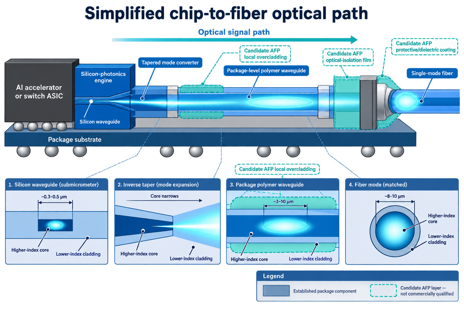
Figure 1. A simplified chip-to-fiber optical path in a photonic package. Core materials, dimensions, and coupling method vary by architecture. Candidate AFP layers are illustrative and do not imply qualification in a commercial CPO platform.
Core, cladding, and why refractive index matters
An optical waveguide usually contains a core with a higher refractive index surrounded by a cladding with a lower refractive index. The difference between the two helps confine light to the core. Refractive index describes how strongly a material slows and bends light; the core-cladding difference influences confinement, bend radius, crosstalk, mode size, coupling behavior, and sensitivity to manufacturing variation. [2]
Commercial AFP families can provide refractive indices roughly in the 1.29-1.34 range in visible-light measurements, depending on polymer chemistry. [10-12] That is unusually low for a solid polymer and can create substantial index contrast against silica, silicon nitride, conventional optical polymers, or photoresist-based waveguide cores.
While a very low-index cladding can strengthen confinement and optical isolation, it can also shrink the optical mode and make coupling to another waveguide or fiber more difficult. Some couplers need a cladding or adhesive whose index is close to another material, not as low as possible. In low-index-contrast systems, small temperature-driven changes in the index of the cladding, substrate, or adhesive can produce meaningful excess loss. [2,9]
The key design question is, ‘What refractive-index profile, thickness, geometry, and thermal behavior produce the required mode and loss budget in this specific stack?’ The AFP material is one design variable in a coupled optical, mechanical, thermal, and manufacturing problem.
Where polymers are entering photonic packages
Package-level polymer waveguides can act as an optical redistribution layer (RDL). Similar to an electrical redistribution layer that reroutes electrical connections, an optical RDL can fan optical channels out from dense photonic chip interfaces toward fibers or other components at the package edge. Polymers are attractive because they can be deposited over large areas, patterned at relatively low temperatures, and formulated with controlled core and cladding indices. [5]
The imec-led program provides a useful modern example. Its demonstrated optical RDL used commercial, matched, UV-patternable EpoCore/EpoClad epoxy materials as the higher-index core and lower-index cladding, respectively, of polymer optical waveguides, not an AFP. The polymer waveguide was integrated with silicon nitride tapers and showed low propagation and transition losses in the O-band (approximately 1260-1360 nm, centered near 1310). [5] IBM has likewise demonstrated high-density single-mode polymer-waveguide interfaces for CPO modules and reported mechanical and thermomechanical reliability testing. [6,7] These results establish that polymer waveguides can perform serious packaging work, but not that an AFP is the best material for the job.
Other architectures use three-dimensional polymer waveguides called photonic wire bonds. These freeform structures bridge misaligned optical chips after the components are placed, reducing the need to position every waveguide facet with sub-micrometer precision beforehand. In a 2012 proof-of-principle demonstration, an SU-8 waveguide core connected silicon waveguides, with an index-matching liquid used to emulate a low-index cladding. The design identified CYTOP as one possible cladding material. The work reported average insertion loss of 1.6 dB across the C-band and multi-terabit-per-second data transmission. [8]
That work shows how an AFP could serve as the low-index cladding around a chip-scale polymer interconnect, but it did not experimentally qualify CYTOP in a packaged device. It leaves unanswered questions about reliability in a current AI CPO product, compatibility with today’s package processes, and equivalence among CYTOP®, Teflon™ AF and CyclAFlor® formulations.
Why AFPs are plausible candidates
Ultra-low refractive index
An AFP cladding can create strong index contrast with many optical core materials. Depending on the architecture, that may improve confinement, reduce leakage into the substrate, lower crosstalk between neighboring channels, or allow a thinner optical-isolation layer. [2,10-12] CYTOP has been used as cladding in photonic wire bonds and long-range surface-plasmon devices [8,9], while Teflon AF has been positioned and demonstrated as a low-index cladding in optical-fiber and optofluidic structures. [10,13]
Optical transparency across relevant wavelengths
Many data-communication links operate near 1310 nm in the O-band or 1550 nm in the C-band. [5,8] AFPs can provide broad optical transparency into the near infrared, but qualification requires the absorption coefficient, extinction coefficient, scatter, fluorescence, and total waveguide loss at the actual wavelength, thickness, cure condition, and optical power. [10-12]
Solution processing and conformal film formation
AFPs are soluble in selected fluorinated solvents and applied as thin films by spin coating, dip coating, spray coating, casting, or other solution processes. [10-12] That processability can be useful for overcladding a patterned waveguide, coating a three-dimensional interconnect, filling selected gaps, or forming an optical-isolation film on a package substrate.
Chemical resistance and dielectric performance
AFPs can resist many chemicals and provide low dielectric constants. [10-12] Chemical resistance may help protect an optical layer during later processing or operation. Low dielectric behavior may be useful near high-speed electrical traces in a mixed optical-electrical package. These are potentially complementary benefits, but each must be tested in the actual stack. A material that is an excellent optical cladding can still fail because it does not adhere, cracks during thermal cycling, contaminates another process, or cannot be patterned with acceptable yield.
The evidence is promising, but it comes from different technology generations
The public evidence falls into three distinct categories.
- Current CPO and optical-I/O evidence: production announcements and recent demonstrations show that optics is moving closer to AI switches and compute packages, and that package-level polymer waveguides can meet demanding optical and reliability targets. The published systems generally use non-AFP polymer systems or do not disclose the polymer chemistry. [1,3-7]
- Direct AFP waveguide evidence: Early photonic-wire-bond work identified CYTOP as a possible low-index cladding, CYTOP has served as cladding in surface-plasmon waveguides, and CYTOP-based all-polymer waveguide devices have operated near 1550 nm. Teflon AF has been used in optofluidic waveguides, while Chemours identifies optical-fiber cladding as an intended application. [8-10,13,14]
- Current AFP platform potential: CYTOP, Teflon AF, and CyclAFlor product literature identifies low refractive index, optical transparency, thin-film processability, and optical cladding or waveguide-related applications. Manufacturer positioning supports technical plausibility but is not proof of customer qualification. [10-12]
In short, AFPs have demonstrated relevant optical functions, including waveguide and optical-device cladding, but their fit for a modern CPO stack has yet to be established commercially. [8,9,13,14]
A proposed AFP opportunity framework
The most credible opportunities are locations where a low-index solid film performs a specific optical or protective job and where solution processing is compatible with the assembly sequence. [2,5,6,8-14]
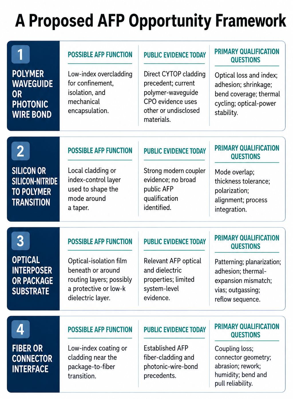
Table 1. Opportunity-screening framework showing potential functions, not claims of current AFP qualification in commercial CPO products.
The coupling layer may be the wrong place for the lowest index
While optical coupling layer may sound like an obvious AFP opportunity, a low-index material inserted in the wrong location could increase loss. At some interfaces, a low-index material helps isolate a waveguide from a substrate or confine the optical mode. At others, a higher-index or index-matched adhesive reduces reflections and expands the mode into the receiving waveguide. [2,5]
This is why the optical design must precede material selection. The stack should be modeled using measured wavelength-dependent optical constants, realistic thickness tolerances, sidewall and surface roughness, temperature-dependent index values, and the expected alignment distribution. [2,5,9] Only then can the designer identify whether to use an AFP as the cladding, an isolation film, a non-optical protective coating, or not at all.
What qualification would need to prove
A credible AFP development program for photonic packaging should begin with a defined optical path, package flow, and reliability target. The material and process would likely need to establish the following [2,5,6,15]:
- Refractive index and extinction coefficient at every operating wavelength and across the required temperature range.
- Propagation, coupling, bend, and transition loss at the actual film thickness, geometry, polarization, and optical power.
- Thickness uniformity, surface roughness, sidewall and corner coverage, pinholes, bubbles, voids, and residual-solvent control.
- Adhesion to the actual core, substrate, metallization, passivation, and neighboring dielectric materials.
- Dimensional and optical stability through deposition, cure, package assembly, reflow or optics-last processing, thermal cycling, humidity, and storage.
- Thermo-optic behavior, cure shrinkage, residual stress, coefficient-of-thermal-expansion mismatch, cracking, and delamination.
- Compatibility with lithography, developers, cleaning agents, plasma treatments, adhesives, underfills, flux residues, and any fluorinated coating solvents.
- High-optical-power durability, photochemical stability, outgassing, extractables, ionic contamination, and particle generation.
- Manufacturing repeatability, inspection methods, repair or rework strategy, supply-chain control, and cost per good package.
Taken together, these requirements mean that AFP qualification must demonstrate that a particular formulation, applied by a defined process and integrated at a specific point in the package flow, delivers stable optical performance without compromising adjacent materials, manufacturing yield, or long-term reliability.
The AI value-chain connection
AI demand is increasing the value of every watt and every millimeter devoted to data movement. Optical interconnects can reduce the distance that the fastest electrical signals must travel and can provide higher bandwidth density over longer reaches. Photonic packaging turns that systems problem into a materials-and-manufacturing problem at the interfaces among chips, waveguides, substrates, and fibers. [1,5]
AFPs connect to this part of the AI value chain through the functional job of managing light. Their low refractive index can help define where the optical mode travels; their transparency can limit absorption; their processability can enable coatings around delicate or three-dimensional structures; and their chemical and dielectric properties may solve adjacent package problems. [10-12]
Conclusion: the package is an optical system, not a collection of materials
Co-packaged optics and related optical-I/O architectures are moving from research into early commercial deployment because AI networks need more bandwidth with lower power and higher connection density. Recent work from IBM, imec, and others shows that package-level polymer waveguides can provide practical bridges among silicon photonics, interposers, and fibers. [3-7]
AFPs bring a rare combination of ultra-low refractive index, broad transparency, chemical resistance, low dielectric constant, and solution processability. [10-12] Direct CYTOP and Teflon AF evidence shows that amorphous fluoropolymers can function as optical claddings and waveguide materials. [9,13,14] The public evidence does not yet show broad AFP adoption in modern AI-focused CPO platforms, and it does not establish that one AFP grade can be substituted for another without requalification.
The near-term opportunity requires evaluating AFPs where a package design needs a very low-index, optically clear, processable solid layer and where the total optical, thermal, mechanical, contamination, and manufacturing budgets can support it.
In the next article, we will follow light beyond the package into specialty fibers and optical sensing, where AFPs may serve as low-index claddings, overcladdings, or chemically resistant optical interfaces in AI and high-performance-computing environments.
Learn More
If you are developing a photonic package, optical interposer, polymer waveguide, or chip-to-fiber interface where refractive index, optical loss, chemical compatibility, or film processing is limiting performance, Chromis Technologies can help evaluate whether a CyclAFlor® amorphous fluoropolymer belongs in the design. Contact us to discuss the optical stack, process conditions, and qualification requirements.
References
- Wang, Y. et al. Co-Designed Silicon Photonics Chip I/O for Energy-Efficient Petascale Connectivity. IEEE Transactions on Components, Packaging and Manufacturing Technology 15(8), 1581-1595 (2025). DOI: 10.1109/TCPMT.2024.3492189
- Weninger, D. et al. Advances in Waveguide-to-Waveguide Couplers for 3D Integrated Photonic Packaging. Light: Science & Applications 15, 17 (2026). DOI: 10.1038/s41377-025-02048-w
- Broadcom Inc. Broadcom Announces Tomahawk 6 – Davisson, the Industry’s First 102.4-Tbps Ethernet Switch with Co-Packaged Optics. October 8, 2025. https://investors.broadcom.com/news-releases/news-release-details/broadcom-announces-tomahawkr-6-davisson-industrys-first-1024.
- NVIDIA Vera Rubin Ramps Into Full Production to Power Agentic AI Factories Worldwide. May 31, 2026. https://nvidianews.nvidia.com/news/vera-rubin-full-production-agentic-ai-factory.
- Van Asch, J. et al. Low-Loss Integration of High-Density Polymer Waveguides with Silicon Photonics for Co-Packaged Optics. Optica 12(6), 821-830 (2025). DOI: 10.1364/OPTICA.559260
- Horibe, A. et al. Co-Packaged Optics Module with Single-Mode Polymer Waveguide. 2025 IEEE International Electron Devices Meeting (IEDM) (2025). DOI: 10.1109/IEDM50572.2025.11353491
- IBM Research. Co-Packaged Optics Can Supercharge Generative AI Computing. December 2024. https://research.ibm.com/blog/co-packaged-optics-to-supercharge-generative-ai-computing.
- Lindenmann, N. et al. Photonic Wire Bonding: A Novel Concept for Chip-Scale Interconnects. Optics Express 20(16), 17667-17677 (2012). DOI: 10.1364/OE.20.017667
- Fan, H.; Berini, P. Thermo-Optic Characterization of Long-Range Surface-Plasmon Devices in Cytop. Applied Optics 52(2), 162-170 (2013). DOI: 10.1364/AO.52.000162
- Teflon AF Amorphous Fluoroplastic Resins: Product Information. https://www.chemours.com/en/-/media/files/teflon/teflon-af-product-info.pdf
- AGC Chemicals Americas. CYTOP Amorphous Fluoropolymer. https://www.agcchem.com/products/high-performance-coatings/cytop/
- Chromis Technologies. CyclAFlor Clear and CyclAFlor Shield Product Information. https://chromistechnologies.com/products/cyclaflor-clear/ and https://chromistechnologies.com/products/cyclaflor-shield/
- Cho, S. H.; Godin, J.; Lo, Y.-H. Optofluidic Waveguides in Teflon AF-Coated PDMS Microfluidic Channels. IEEE Photonics Technology Letters 21(15), 1057-1059 (2009). DOI: 10.1109/LPT.2009.2022276.
- Takenobu, S. et al. All-Polymer 8×8 AWG Wavelength Router Using Ultra Low Loss Polymer Optical Waveguide Material (CYTOP). OFC/NFOEC 2008, paper JWA32 (2008). DOI: 10.1109/OFC.2008.4528185
- Suda, S. et al. High-Power Stability and Reliability of Polymer Optical Waveguide for Co-Packaged Optics. Journal of Lightwave Technology 43(10), 4903-4912 (2025). DOI: 10.1109/JLT.2025.3543339
Frequently Asked Questions (FAQs)
What is photonic packaging?
Photonic packaging is the integration of photonic chips with electronic chips, waveguides, fibers, package substrates, electrical connections, and thermal-management structures. It includes the optical interfaces and assembly processes needed to move light reliably into, out of, and among components.
What is co-packaged optics?
Co-packaged optics, or CPO, places optical engines close to a network-switch or compute ASIC on a common package or substrate. Shortening the highest-speed electrical path can reduce signal loss and power consumption while increasing bandwidth density.
What is an optical redistribution layer?
An optical redistribution layer routes optical channels across an interposer or package substrate, much as an electrical redistribution layer reroutes electrical connections. Polymer, glass, or silicon nitride waveguides may be used, depending on the architecture.
Why does a waveguide need cladding?
A waveguide core normally has a higher refractive index than the surrounding cladding. The index difference helps confine light to the core and influences mode size, bend loss, crosstalk, coupling, and routing density.
Why might amorphous fluoropolymers be useful as claddings?
AFPs can provide unusually low refractive index, optical transparency, chemical resistance, and solution-based film formation. Those properties may be useful where a design needs strong optical isolation or a conformal low-index layer around a waveguide.
Does a lower refractive index always improve optical coupling?
No. A lower cladding index may strengthen confinement but shrink the optical mode, which can worsen overlap with a fiber or neighboring waveguide. Some interfaces need index matching rather than the lowest possible index.
Are AFPs already used in commercial AI co-packaged optics?
Public research shows CYTOP and Teflon AF in relevant waveguide and cladding roles, and current CPO work shows strong interest in polymer waveguides, but the evidence reviewed here does not establish broad AFP qualification or adoption in current commercial AI-focused CPO platforms.
Could CyclAFlor replace CYTOP or Teflon AF in a photonic package?
Possibly, but the specific CyclAFlor grade, molecular weight, functional group, solvent, coating process, cure, adhesion, wavelength-dependent optical constants, and package reliability would need to be tested in the actual stack.
What is the biggest technical risk for an AFP in photonic packaging?
There is no single risk. The main challenge is meeting the complete system budget: optical loss, index stability, adhesion, stress, thermal cycling, contamination control, process compatibility, manufacturability, and reliability at the same time.