

Part 4 of a Series on Amorphous Fluoropolymers in the AI Value Chain
Amorphous fluoropolymers may offer contamination resistance, optical clarity, low refractive index, chemical durability, and thin-film processability at selected semiconductor optical interfaces.
The previous article in this series examined amorphous fluoropolymer (AFP) films used as membranes in deep-ultraviolet (DUV) pellicles. A pellicle protects a photomask or reticle by holding particles away from the patterned surface and outside the focal plane.
Now we’ll move one layer closer to the pattern itself to examine whether an AFP coating could help protect a reticle surface from contamination and whether the same family of low-refractive-index, optically clear coatings might have useful roles on selected surfaces in semiconductor inspection and optical metrology systems.
U.S. Patent 6,566,021 “Fluoropolymer-Coated Photomasks for Photolithography” (2003) describes the use of Teflon™ and CYTOP® AFP coatings applied directly over a photomask pattern to protect it from contamination, scratches, and chemical degradation during DUV exposure processes in chip fabrication. AGC lists anti-fouling coatings for photomasks among the applications for CYTOP. Published research also establishes that Teflon AF and CYTOP can form low-index optical coatings. The public evidence, however, does not establish that AFP reticle coatings or AFP coatings inside semiconductor inspection and metrology tools are broadly used or qualified in modern high-volume manufacturing.
For these potential use cases, a coating must protect a critical surface while remaining optically and dimensionally inconspicuous. If it changes the pattern’s transmission, phase, reflectivity, defect signature, or measured position, it may create a larger problem than the one it was intended to solve.
How are photomasks, reticles, pellicles, and coatings related?
A photomask is an intricately patterned plate used to transfer a circuit image during semiconductor lithography. In advanced projection lithography, the mask is commonly, though somewhat imprecisely, called a reticle. The patterned surface may contain opaque absorber features, phase-shifting structures, or, in the case of extreme ultraviolet (EUV) lithography, a reflective multilayer stack and absorber pattern.
A pellicle is a separate thin membrane suspended on a frame above the reticle. It protects the patterned surface without being directly applied to it.
A reticle coating is a film applied directly to the pattern, the substrate, or another surface of the mask or reticle.
An inspection or optical metrology coating is applied to a window, sensor cover, reference surface, non-imaging optic, or another component within the system.
While these features are related, they are very different technically. The coating on a reticle can affect the image that prints on the wafer. A coating in an inspection system can affect which defects are detected. A coating in a metrology system can affect what dimensions or positions are measured.
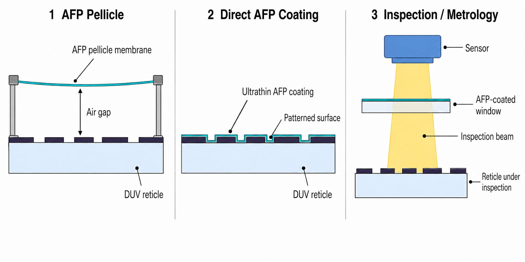
The pattern must survive more than exposure
Reticle contamination from particles, organic residues, ionic contaminants, airborne molecular contamination, and photochemically generated haze can all degrade mask performance. Research on 193 nm ArF reticles has documented haze formation on mask surfaces and shown that environmental exposure, surface chemistry, residual ions, humidity, cleaning, and accumulated ultraviolet dose can interact in complicated ways. Haze can reduce transmission or create printable defects, and some contamination can evade routine through-pellicle inspection. [1–3]
Photomask cleaning is necessary and the process must remove contamination without shifting critical dimensions, damaging absorber or anti-reflective layers, disturbing small assist features, or changing the phase and transmission of a phase-shift mask. [2] Repeated cleaning can also consume mask life, require pellicle removal and replacement, add inspection cycles, and interrupt production.
Inspection and metrology provide the control loop. Reticle inspection finds particles, pattern defects, and changes that could print on the wafer. Optical metrology measures quantities such as critical dimension, transmission, phase, registration, overlay, and pattern placement. Modern mask inspection also uses computational methods to connect a measured defect to its likely printability. [4] The reticle is repeatedly inspected, measured, transported, stored, exposed, cleaned, and requalified.
A useful protective coating must be compatible with that entire lifecycle.
What would a direct reticle coating have to do?
The concept is to place a chemically inert, low-surface-energy film between the environment and the patterned reticle. In principle, the coating could reduce wetting or adhesion by some contaminants, make selected residues easier to remove, and protect the underlying pattern from reactive species or cleaning chemistry. To succeed, however, the coating would have to satisfy all of the following:
- Transmit the relevant DUV or inspection wavelength with acceptably low absorption, haze, and scatter.
- Maintain tightly controlled thickness and refractive index across the full reticle area.
- Avoid changing mask phase, transmission, reflectivity, critical dimensions, edge placement, or defect printability beyond the process budget.
- Adhere to the actual substrate and pattern materials without voids, pinholes, edge bead, delamination, or trapped contamination.
- Generate essentially no particles, outgassing, extractables, mobile ions, or other contamination.
- Survive ultraviolet dose, thermal cycling, storage, transport, pellicle mounting, inspection, and approved cleaning processes.
- Remain compatible with repair, recertification, and the customer’s existing reticle-handling workflow.
The list explains why a good coating material is only the starting point. The previously-cited U.S. patent describes photomasks covered by Teflon AF and CYTOP films intended to reduce contamination at the mask surface. That is meaningful evidence that the concept is technically grounded but is not proof of present-day commercial adoption. The real product is a qualified mask stack and process.
Why are amorphous fluoropolymers plausible candidates?
Several properties make them technically interesting for contamination-sensitive optical surfaces.
Optical clarity and wavelength-specific absorption
Unlike many crystalline or semicrystalline fluoropolymers, certain AFPs can form highly transparent films. Detailed spectroscopic-ellipsometry and transmission measurements of Teflon AF grades show that refractive index and absorption depend on polymer composition and wavelength. [5] To qualify for commercial use, the film must be characterized at the actual exposure, inspection, or metrology wavelength and at the actual thickness.
Ultra-low refractive index
AFPs are among the lowest-refractive-index solid polymers. A low-index film can reduce reflection when its index and thickness are properly matched to the substrate and wavelength. Teflon AF has been demonstrated as a solution-processed antireflective optical coating, and CYTOP coatings have reduced reflection loss on sensitive optical crystals. [6, 8, 9] These studies do not prove performance on a photomask or inside a semiconductor metrology tool, but they do establish that AFPs can function as engineered optical layers, not merely as hydrophobic topcoats.
Chemical resistance and low surface energy
AFPs can offer strong chemical resistance and low surface energy. Those properties may reduce interactions with water, oils, and some contaminants, while helping a thin film survive selected solvents or cleaning environments. ACG lists anti-fouling coatings for photomasks as a CYTOP application. [12]
Particle adhesion depends on particle chemistry, electrostatics, humidity, surface roughness, contact area, and environmental history. Haze can be a photochemical growth process rather than simple wetting. A hydrophobic surface may help with one mechanism and do little – or something undesirable – with another.
Thin-film processability
Teflon AF, CYTOP, and CyclAFlor® AFPs are soluble in selected fluorinated solvents and applied by spin, dip, spray, or related coating methods. This solution processability enables submicron films over large optical substrates. It also creates process variables – solvent purity, solution filtration, substrate preparation, wetting, cure conditions, edge-bead control, residual solvent, thickness uniformity, and defect density – to be optimized for qualification and production.
There is real, but uneven, technical evidence
Support for AFPs in this application area falls into three tiers:
- Direct photomask evidence: a U.S. patent describes amorphous fluoropolymer-coated photomasks, and AGC identifies CYTOP for photomask anti-fouling coatings. [11, 12]
- General optical-coating evidence: peer-reviewed studies demonstrate low-index AFP films, antireflective behavior, and solution processing on optical substrates. [5–9]
- Current platform potential: Chemours positions Teflon AF for low-index optical coatings and Chromis positions CyclAFlor® for protective and optical coatings. [13, 17]
While historical evidence involving Teflon AF or CYTOP supports the AFP material class, application qualification involves variables comprising polymer composition, functional groups, molecular weight, solvent, additives, purity, coating process, and cure that can all change optical and surface performance.
A proposed AFP adoption framework based on available technical evidence
One way to screen AFP coating opportunities might be by location and function.
 Inspection and optical metrology are plausible but unproven adjacencies
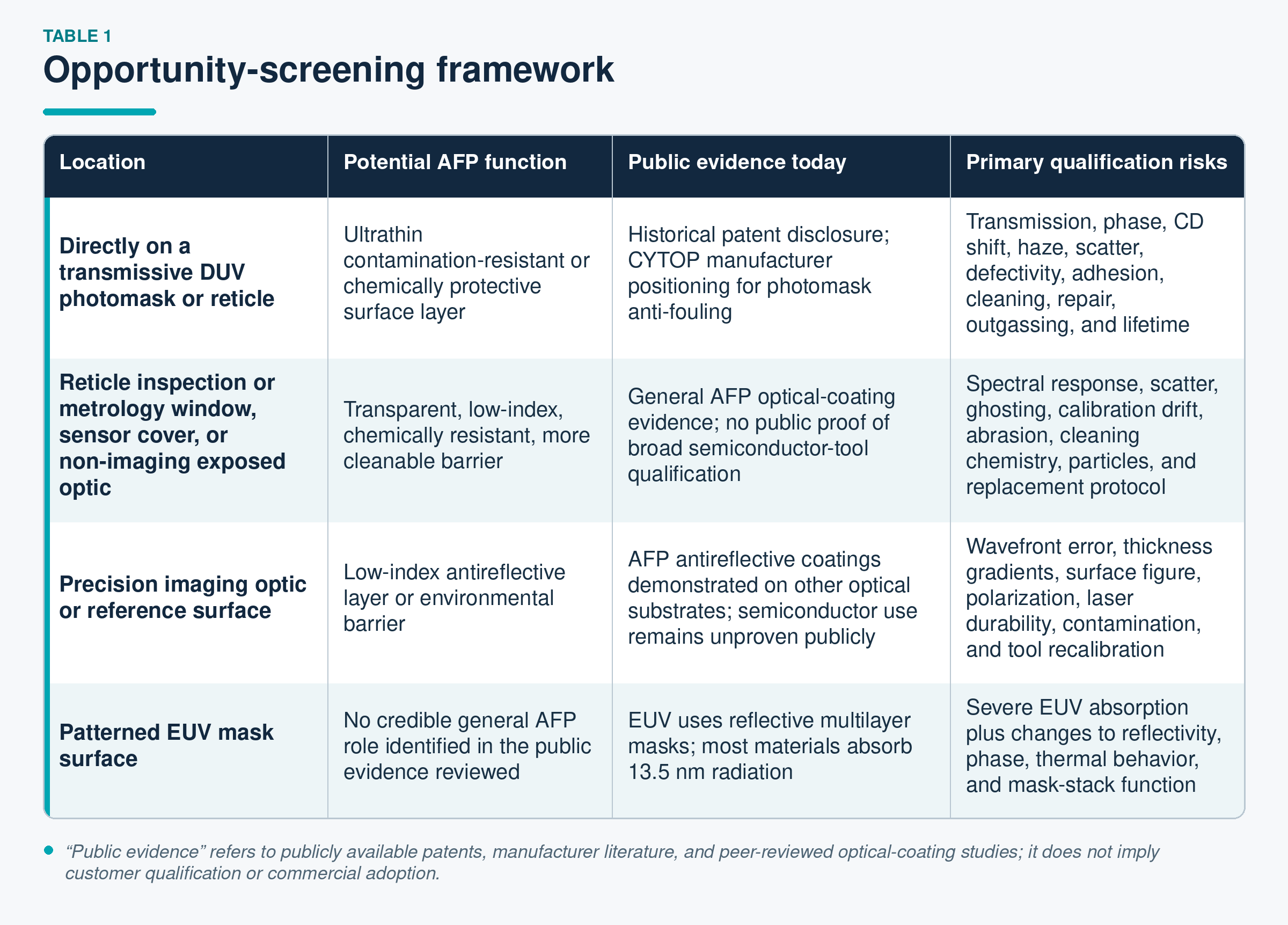
Reticle inspection systems use optical and computational methods to detect pattern defects, particles, and changes that could print on a wafer. Mask metrology systems measure pattern placement, registration, critical dimensions, phase, and related parameters with extreme precision. Commercial systems support optical and EUV masks and, in some cases, sub-nanometer repeatability or accuracy. [14, 15]
These tools contain many surfaces, but do not present one coating opportunity. An exposed protective window or replaceable sensor cover may tolerate a coating concept that would be unacceptable on a precision imaging optic. A non-imaging barrier may primarily need optical transmission, chemical resistance, low scatter, and cleanability. An imaging surface may also have strict requirements for wavefront quality, polarization behavior, spectral uniformity, laser-induced damage resistance, and calibration stability.
An AFP coating could be worth evaluating where a surface is difficult or expensive to clean, where chemical exposure threatens an optical substrate, or where a very low-index layer can be designed into the optical stack. But the coating must improve the total tool problem. A film that is easier to clean but adds scatter, fluorescence, ghost reflections, or measurement drift is not an improvement.
Low refractive index can help if designed into the stack
A low-refractive-index film can act as a single-layer antireflective coating when its refractive index and optical thickness create destructive interference between reflected waves. AFPs are attractive because their refractive indices are lower than those of most solid polymers and many conventional coating materials. Research has demonstrated this behavior on high-power-laser and nonlinear-crystal optical surfaces. [6, 8, 9]
Whether a lower index delivers the desired performance depends on the substrate index, coating thickness, angle of incidence, polarization, wavelength range, surface roughness, and the rest of the optical stack. Broadband inspection systems may need a multilayer or graded solution. DUV systems may encounter composition-dependent absorption near the polymer’s optical edge. Metrology systems may care more about phase stability and uniformity than about a modest gain in transmission.
What qualification would need to prove
A credible AFP coating program for reticles, semiconductor inspection, or optical metrology should begin with the actual surface, wavelength, optical path, contamination mechanism, cleaning method, and error budget. The qualification plan might include:
- Optical constants (n and k) at every relevant exposure, inspection, and metrology wavelength.
- Transmission, reflectivity, phase, polarization response, fluorescence, haze, and scatter at the actual film thickness.
- Full-area thickness uniformity, surface roughness, pinholes, edge bead, coating defects, and pattern-topography coverage.
- Adhesion to quartz, absorber, phase-shift, anti-reflective, capping, or other actual stack materials.
- Particle-addition testing, outgassing, extractables, mobile ions, nonvolatile residue, and airborne molecular contamination behavior.
- Contaminant adsorption and release testing using the relevant particles, organics, acids, bases, humidity, and ultraviolet dose.
- Compatibility with pellicle mounting, reticle pods, inspection recipes, repair methods, and approved cleaning chemistries.
- Accelerated ultraviolet exposure, thermal aging, storage, transport simulation, and repeated cleaning.
- Impact on defect detectability, false positives, false negatives, printability assessment, registration, critical-dimension measurement, and calibration drift.
- A removal or rework path that does not damage the reticle or optical component.
- Manufacturing repeatability, supply-chain control, cost, and ownership of the added process risk.
Surface modification adds another complication. Plasma treatment or primers may improve adhesion or alter wetting, but they can also change roughness, chemistry, thickness, and optical behavior. Research on oxygen-plasma-treated Teflon AF1600 illustrates how strongly processing conditions can change AFP surface topography and wetting properties. [10] The process and the polymer must be qualified together.
The AI value-chain connection
AI demand increases the need for advanced processors, high-bandwidth memory, and the semiconductor capacity required to produce them. Those chips depend on reticles that preserve pattern fidelity and on inspection and metrology systems that detect defects before they become repeated yield losses. AFPs connect to the AI value chain at this upstream manufacturing layer. They are specialty optical and protective materials that may help solve selected contamination, surface, and interface problems inside the manufacturing infrastructure behind AI chips.
Conclusion: the coating must protect without becoming part of the pattern
Photomasks and reticles are among the most consequential reusable components in semiconductor manufacturing. A defect or contaminant on the wrong surface can be repeated across many die and many wafers. Inspection and optical metrology exist to find and measure those risks before they become yield loss.
Amorphous fluoropolymers offer a technically relevant combination of optical clarity, ultra-low refractive index, chemical resistance, low surface energy, and solution-based thin-film processability. Historical patent disclosures and current manufacturer literature support the concept of AFP anti-fouling coatings for transmissive photomasks. Peer-reviewed studies support the use of AFPs as low-index optical coatings.
The case for AFP coatings inside semiconductor inspection and metrology systems is more exploratory. Selected windows, sensor covers, reference surfaces, or non-imaging optics may offer logical starting points. Precision imaging optics impose a much higher bar.
The opportunity is to identify the few contamination-sensitive interfaces where an ultrathin AFP film may improve the entire system. The reticle carries the pattern. Inspection finds what should not be there. Metrology measures what must be exactly right. The coating earns a place only if all three can effectively forget it is there.
Learn More
If you are evaluating an optically clear, low-refractive-index, chemically resistant coating for a photomask, reticle-adjacent component, optical window, or metrology interface, we would welcome a conversation about the application requirements and qualification path. Contact Chromis Technologies to learn more about CyclAFlor® materials, coating options, and development support.
References
Research papers and technical proceedings
[1] Johnstone, E.; Dieu, L.; Chovino, C.; Reyes, J.; et al. “193-nm Haze Contamination: A Close Relationship Between Mask and Its Environment.” Proceedings of SPIE, Vol. 5256, 2003. DOI: 10.1117/12.518262.
[2] Graham, M.; McDonald, A. “Photomask Cleaning Process Improvement to Minimize ArF Haze.” Proceedings of SPIE, Vol. 6792, 2008, 67920D. DOI: 10.1117/12.798592.
[3] Kishkovich, O.; Kielbaso, T.; Halbmaier, D. “Reticle Haze Control: Global Update and Technology Roadmap.” Proceedings of SPIE, Vol. 7638, 2010, 763819. DOI: 10.1117/12.848432.
[4] Pang, L.; Peng, D.; Hu, P.; Chen, D.; He, L.; Li, Y.; Satake, M.; Tolani, V. “Computational Metrology and Inspection (CMI) in Mask Inspection, Metrology, Review, and Repair.” Advanced Optical Technologies, 2012, 1(4), 299–321. DOI: 10.1515/aot-2012-0127.
[5] Yang, M. K.; French, R. H.; Tokarsky, E. W. “Optical Properties of Teflon® AF Amorphous Fluoropolymers.” Journal of Micro/Nanolithography, MEMS, and MOEMS, 2008, 7(3), 033010. DOI: 10.1117/1.2965541.
[6] Bazin, N. J.; Andrew, J. E.; McInnes, H. A. “Formation of Teflon AF Polymer Thin Films as Optical Coatings in the High-Peak-Power Laser Field.” Proceedings of SPIE, Vol. 3492, 1999, 964–969. DOI: 10.1117/12.354247.
[7] Zhang, H.; Weber, S. G. “Teflon AF Materials.” In Fluorous Chemistry, Topics in Current Chemistry, Vol. 308, Springer, 2012, pp. 307–337. DOI: 10.1007/128_2011_249.
[8] Uchida, H.; Koyama, C.; Takagi, T.; Wang, P.; Kamei, T.; Kawase, K.; Takeya, K. “Antireflection Coating on Organic Nonlinear Optical Crystals Using Soft Materials.” Applied Physics Letters, 2019, 115, 231107. DOI: 10.1063/1.5126462.
[9] Uchida, H.; Kawauchi, T.; Otake, G.; et al. “Optical Thin Film Coated Organic Nonlinear Crystal for Efficient Terahertz Wave Generation.” Scientific Reports, 2022, 12, 15082. DOI: 10.1038/s41598-022-17893-7.
[10] Xiang, Y.; Fulmek, P.; Sauer, M.; Foelske, A.; Schmid, U. “Characterization of Surface Modifications in Oxygen Plasma-Treated Teflon AF1600.” Langmuir, 2024, 40, 4779–4788. DOI: 10.1021/acs.langmuir.3c03639.
Technical, industry, and product sources
[11] U.S. Patent No. 6,566,021 B2, “Fluoropolymer-Coated Photomasks for Photolithography,” issued May 20, 2003. https://patents.google.com/patent/US6566021B2/en. Used as historical evidence of direct AFP photomask-coating concepts; a patent is not proof of commercial adoption.
[12] AGC Chemicals, “CYTOP™ Amorphous Fluoropolymers.” https://www.agcchem.com/products/high-performance-coatings/cytop/. Lists anti-fouling coatings for photomasks, anti-reflective coatings, and relevant AFP properties.
[13] Chemours, “Teflon™ AF Amorphous Fluoropolymer Resins.” https://www.teflon.com/en/products/resins/amorphous-fluoropolymer. Used for optical-coating positioning, low refractive index, chemical resistance, UV stability, and solution processability.
[14] KLA, “Reticle Manufacturing.” https://www.kla.com/products/reticle-manufacturing. Used for current reticle inspection, defect-control, and pattern-registration applications.
[15] ZEISS Semiconductor Manufacturing Technology, “Photomask Metrology Solutions.” https://www.zeiss.com/semiconductor-manufacturing-technology/products/photomask-solutions/mask-metrology.html. Used for mask registration, overlay, and sub-nanometer metrology context.
[16] ASML, “Lenses & Mirrors—Lithography Principles.” https://www.asml.com/technology/lithography-principles/lenses-and-mirrors. Used for the absorption of EUV by most materials and the need for multilayer reflective optics.
[17] Chromis Technologies, “CyclAFlor® Shield.” https://chromistechnologies.com/products/cyclaflor-shield/. Used for current CyclAFlor positioning in transparent protective and low-index optical coatings; application-specific qualification remains necessary.
Frequently Asked Questions (FAQs)
What is the difference between a photomask and a reticle?
Both terms describe the patterned component used to transfer a circuit image during semiconductor lithography. “Photomask” is the broader term; “reticle” is commonly used for masks in projection lithography systems. In either case, contamination or pattern defects can be repeated across many die and wafers.
Is a reticle coating the same thing as a pellicle?
No. A pellicle is a thin membrane suspended above the reticle to keep particles away from the focal plane. A reticle coating is a film applied directly to the mask, pattern, substrate, backside, or another reticle surface. The two approaches may complement each other, but they create different optical and contamination-control requirements.
What is reticle contamination?
Reticle contamination includes particles, organic residues, ionic materials, airborne molecular contaminants, and photochemically generated deposits on a photomask or reticle. Contamination can change transmission, create haze, interfere with inspection, or produce repeated printable defects that reduce semiconductor yield.
What is photomask or reticle haze?
Reticle haze is a contaminant film or crystal growth that develops on a photomask surface, often through interactions among residual chemicals, humidity, airborne molecular contamination, and ultraviolet exposure. Haze has been a significant issue in 193 nm ArF lithography because it can reduce mask transmission or create defects.
Can an AFP coating replace a pellicle?
Generally, no. A pellicle physically holds particles away from the patterned surface. An AFP coating may reduce selected surface interactions or protect the underlying material, but it does not move particles outside the focal plane. A direct reticle coating should be considered a possible complementary strategy, not a universal pellicle replacement.
Why might amorphous fluoropolymers be useful as reticle protective coatings?
Amorphous fluoropolymers can combine optical clarity, ultra-low refractive index, chemical resistance, low surface energy, and solution-based thin-film processability. That combination may support an ultrathin contamination-resistant or chemically protective coating on selected transmissive DUV photomask surfaces, provided the coating does not alter lithographic performance.
Are AFP photomask coatings already used commercially?
Public information supports the concept but does not establish broad current use. A granted U.S. patent describes amorphous fluoropolymer-coated photomasks, and AGC lists CYTOP for anti-fouling photomask coatings. Publicly available evidence is much thinner on current high-volume-manufacturing adoption, customer qualifications, and tool-specific use.
What is the difference between semiconductor inspection and optical metrology?
Inspection primarily identifies defects, particles, or anomalies that may affect yield. Optical metrology measures quantities such as critical dimension, phase, transmission, registration, overlay, and pattern placement. Some systems combine inspection, measurement, imaging, and computational analysis, but the technical questions remain different: inspection asks what is wrong; metrology asks how much and where.
Where could AFP coatings fit in semiconductor inspection and metrology equipment?
Possible evaluation points include exposed optical windows, replaceable sensor covers, non-imaging optical barriers, or selected reference surfaces that need low reflection, chemical resistance, cleanability, or contamination control. Coatings on precision imaging optics face a much higher qualification burden because even small changes in wavefront, scatter, phase, or spectral response can affect measurement accuracy.
Can an amorphous fluoropolymer act as an anti-reflective coating?
Yes, in suitable optical designs. Teflon AF and CYTOP have been demonstrated as low-refractive-index antireflective coatings on selected optical substrates. The result depends on coating index, thickness, substrate index, wavelength, angle, polarization, and surface quality. Low refractive index alone does not guarantee low reflection.
Does low surface energy mean particles will not stick?
No. Low surface energy can reduce wetting and adhesion for some liquids and contaminants, but particle attachment also depends on electrostatics, humidity, surface roughness, particle chemistry, contact area, and handling history. Reticle haze may involve photochemical growth rather than simple adhesion. Anti-fouling performance must be tested against the actual contamination mechanism.
Are AFP coatings suitable for EUV photomasks?
A conventional AFP film should not be assumed suitable for the patterned surface of a production EUV mask. EUV uses 13.5 nm radiation, which is strongly absorbed by most materials, and the mask is a carefully engineered reflective multilayer optic. Any added film could change reflectivity, phase, absorption, or thermal behavior. Direct actinic data and mask-stack qualification would be essential.
What does qualification of a photomask coating require?
Qualification can include wavelength-specific optical constants, transmission, phase, reflectivity, haze, scatter, film uniformity, adhesion, particle addition, outgassing, extractables, cleaning compatibility, ultraviolet durability, thermal aging, repair compatibility, defect detectability, printability, and process repeatability. The coating must be proven as part of the complete reticle and tool workflow.
Is CyclAFlor® already qualified for reticle, inspection, or optical metrology coatings?
CyclAFlor is Chromis Technologies’ current AFP platform, supporting a product family positioned for transparent protective and low-index optical coatings. Historical evidence involving Teflon AF and CYTOP supports the broader AFP material class, but it does not automatically qualify CyclAFlor for a specific reticle or metrology application. Customer-specific testing is required.
How do AFP reticle and metrology coatings connect to artificial intelligence?
AI systems require advanced processors and high-bandwidth memory. Those chips depend on semiconductor lithography, photomasks, reticle inspection, optical metrology, and contamination control. AFPs connect to the AI value chain through this upstream manufacturing infrastructure—not because they are broadly used as generic “AI materials.”
What will the next article in this series cover?
Part 5 will examine low-refractive-index claddings and optical coupling layers for photonic packaging and optical interconnects—an emerging area where AFP optical clarity, ultra-low refractive index, and thin-film processability may help manage light at chip, interposer, waveguide, and fiber interfaces.